This thread has been locked.

If you have a related question, please click the "Ask a related question" button in the top right corner. The newly created question will be automatically linked to this question.

CCS/ADS1232: Problem in measuring data from ADS1232

Part Number:

Tool/software: Code Composer Studio

Hi,

I have a custom board with ads1232 associated with a loadcell ,the digital values outputted from ADS1232 is measured by MSP430G2533.Now i just tried to observe data from ADS1232 with different clock provided from MSP430

1.  Is there any suggestion about SCLK( i used 1ms to 10ms clock for one bit data in SCLK pin ,if reduce clock period i can detect small changes but doesn't get a constant value (167777215,16438215 etc).similarly there is no constant offset value )

2.what is the offset value that we obtained normally  from ads1232 (without applying weight)?

3.Does the design need an external crystal connection in XTAL2 pin?

4.if the data is ready i start read data ,does the data get in rising edge of the clock?,does the second bit data receive when i provide another high low to the sclk pin (is it available in the rising edge of the sclk )?

5.i just provide 25 clock to the sclk pin ,as per the data sheet we expect that the data pin must be high but here i didn't get this why?,how to read continuous data from ads1232(please explain)?

6.What is the necessary delay between two set of 24 bit data?(is there any minimum or maximum) .

7.is there any sample code to obtain data from ads1232 ?

Aju

  • Hi Aju,

    See my responses below.

    Best regards,

    Bob B

    Aju s said:

    Part Number: ADS1232

    Tool/software: Code Composer Studio

    Hi,

    I have a custom board with ads1232 associated with a loadcell ,the digital values outputted from ADS1232 is measured by MSP430G2533.Now i just tried to observe data from ADS1232 with different clock provided from MSP430

    1.  Is there any suggestion about SCLK( i used 1ms to 10ms clock for one bit data in SCLK pin ,if reduce clock period i can detect small changes but doesn't get a constant value (167777215,16438215 etc).similarly there is no constant offset value ) [Bob B] Note Figure 34 on page 19 of the ADS1232 datasheet that shows the timing information for the ADS1232.  The t3 time shows that the minimum high or low time for the SCLK which must be at least 100ns, or 200ns for a full period. The maximum frequency for the SCLK is 5MHz. Obviously the SCLK can be a lower frequency, but the SCLK frequency must be fast enough to collect all 24 bits of data for each conversion period.  The SCLK frequency must also be fast enough so that any other processes within the control loop can also take place.  If your clock is 1ms, or 10ms, it is not possible to collect all 24 bits of the data within one conversion period (10sps is 100ms period and 80sps is 12.5ms).  I do not know what frequency the MSP430 is operating at, but if you target a 1 to 2 MHz SCLK frequency that should work for you.

    Also you mention that the data is not a constant value.  Unfortunately you will never see a constant output for a valid input voltage due to noise and quantization error.  See the noise tables on page 5 of the ADS1232 datasheet.  Although the ADS1232 is able to resolve to the 24-bit level, the noise will prevent you from seeing this resolution noise-free.

    2.what is the offset value that we obtained normally  from ads1232 (without applying weight)? [Bob B] The offset is given in the electrical characteristics table on page 3 of the ADS1232 datasheet.  The offset can vary quite a bit from part to part, so it is suggested to use the offset calibration which is initiated with 26 SCLKs.  If you connect a load cell to the input, there will be some offset error of the load cell too which should also be considered.

    3.Does the design need an external crystal connection in XTAL2 pin? [Bob B] XTAL2 pin is only used if an external crystal is used. Most often the internal clock oscillator is used with the ADS1232 which is accomplished by connecting the XTAL1 pin to ground.  An external clock can also be used and applied to the XTAL1 pin.  In either of these cases the XTAL2 pin can be left floating.

    4.if the data is ready i start read data ,does the data get in rising edge of the clock?,does the second bit data receive when i provide another high low to the sclk pin (is it available in the rising edge of the sclk )? [Bob B] Again I refer you to Figure 34.  The SPI mode of operation is mode 1 where the SCLK normally dwells low, and the data changes (shifts out) on the rising edge of SCLK and is latched (valid) on the falling edge of SCLK.  The data are shifted out in a serial manner MSB first with each clock shifting out one bit of the data.  24 SCLKs are required to capture all the data.

    5.i just provide 25 clock to the sclk pin ,as per the data sheet we expect that the data pin must be high but here i didn't get this why?,how to read continuous data from ads1232(please explain)? [Bob B] Figure 35 in the ADS1232 datasheet shows the action of the 25th clock.  The LSB of the data can be either high or low.  The signal for end of the conversion period is a high to low transition on the DRDY\DOUT pin which is the update period for the data to be placed into the output shift register.  This period is approximately 39us which is very difficult to capture in a polling loop.  An interrupt can be used, but often only a polling of the pin is used.  Let's say you are using the polling method which basically looks periodically for a low on DRDY\DOUT.   If you only use 24 SCLKs to read the data, the last bit could be either a high or a low.  There will be no issues if the last bit is high, but if the last bit is already low you may miss entirely the new result, or capture invalid data and start an offset calibration.  So it is always best to force the DRDY\DOUT pin high and then poll for a low state.

    6.What is the necessary delay between two set of 24 bit data?(is there any minimum or maximum) . [Bob B] This relates somewhat to the answer in question 1.  New data are available depending on the state of the SPEED pin (either 10sps or 80sps).  You should only attempt to read data after new data are available and you should make sure all data are read out completely before the ADS1232 updates the output shift register with new results.

    7.is there any sample code to obtain data from ads1232 ? [Bob B] There is some example code for the ADS1232REF which can be downloaded from our ftp site.  This code is a little hard to follow as it uses freeRTOS and is not using a single simple process loop.  The code uses a lot of macros too that may be somewhat difficult to understand.  In particular you may find the ADS1232.c and .h the most helpful.

    ftp://ftp.ti.com/pub/data_acquisition/ADS123xREF/ADS123x_CDROM/Firmware/Firmware_Source_Code/Source_for_123XREF_firmware-1.1.0d.zip

    Aju

  • Hi BOB,

    Thanks for your great support & valuable information .

    Aju
  • Hi BOB, 
    1.what is the value that we obtained in no load condition ?is it a minimum or maximum?

    2.i obtained a 24 bit value from ads1232 in each time when there is no load applied but the first 12 bit where same but the next 12 bit entirely changed in each time why ?(i just provide clock and probed data out through DSO)

    3.When i apply load there will also have same change (when we apply a weight the value goes down and when we release it value goes beyond no load condition values,why this happends??

    Aju

  • Hi Aju,

    Seem my responses below.

    Best regards,

    Bob B

    Aju s said:

    Hi BOB, 
    1.what is the value that we obtained in no load condition ?is it a minimum or maximum? [Bob B] I will assume that when you say no load you are referring to a no load on the load cell that is powered and connected the ADS1232.  The load cell is basically a Wheatstone bridge and with no load  will be in a balanced state.  The output of the bridge in a balanced state is 0V with a common-mode voltage at mid-excitation supply.  However there may be some offset which can be either negative or positive.  The ADS1232 outputs code in binary 2's complement where the positive values range from 0 (0x000000) to positive full-scale (0x7FFFFF) and negative codes ranging from -1 (0xFFFFFF) to negative full-scale (0x800000).

    2.i obtained a 24 bit value from ads1232 in each time when there is no load applied but the first 12 bit where same but the next 12 bit entirely changed in each time why ?(i just provide clock and probed data out through DSO) [Bob B] I talked about this in my first response.  This is noise.  The noise tables are given in the datasheet.  You can also have external noise from EMI/RFI sources.  The bottom line is that even though the ADS1232 can resolve to 24-bits does not mean the output will be 24-bits noise-free.

    3.When i apply load there will also have same change (when we apply a weight the value goes down and when we release it value goes beyond no load condition values,why this happends?? [Bob B] It is difficult to answer a question like this without more specific information.  Do you have screen shots showing the data?  What is the capacity of the load cell?  What is the sensitivity of the load cell?  What are you expecting and what are you getting back as data values?
     
    Aju

  • Hi Bob,

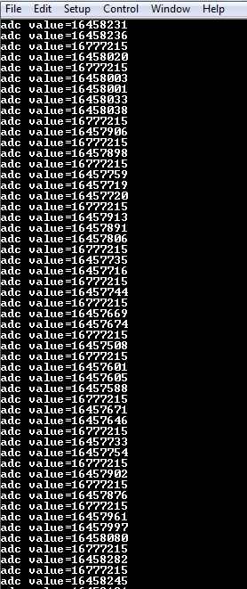
    thanks for your valuable information.here i post my data that i obtained in no load condition.Capacity of the loadcell is 0-25 lbf.(FX1901)

    Aju

  • Hi Aju,

    You are not sign-extending your values from 24 bit to a 32 bit signed value. For example 16777215 is actually 0xFFFFFF as a 24-bit value, but because it is binary 2's complement you must sign-extend the value so that instead of the 32-bit signed integer being 0x00FFFFFF, you make it 0xFFFFFFFF. If bit 23 is a '1' then you must make the most significant 8 bits also a '1'.

    Best regards,
    Bob B