This thread has been locked.

If you have a related question, please click the "Ask a related question" button in the top right corner. The newly created question will be automatically linked to this question.

ADS1015: i2c protocol questions

Part Number: ADS1015

I'm working to build a LabVIEW interface for the TI ADS1015 analog to digital converter.  This is a teaching project, so the hardware is on the cheap.  LabVIEW uses an Arduino as an i2c interface for the ADS1015.  The LINX labview module provides basic i2c communication function via the Arduino Uno's built-in SCL ans SDA pins.  

I'm using the ADS1015 on a breakout board from Adafruit.  The device is set up with i2c address of 1001000_2=0x48=72_10  (LabVIEW specifies byte addresses as unsigned ints).

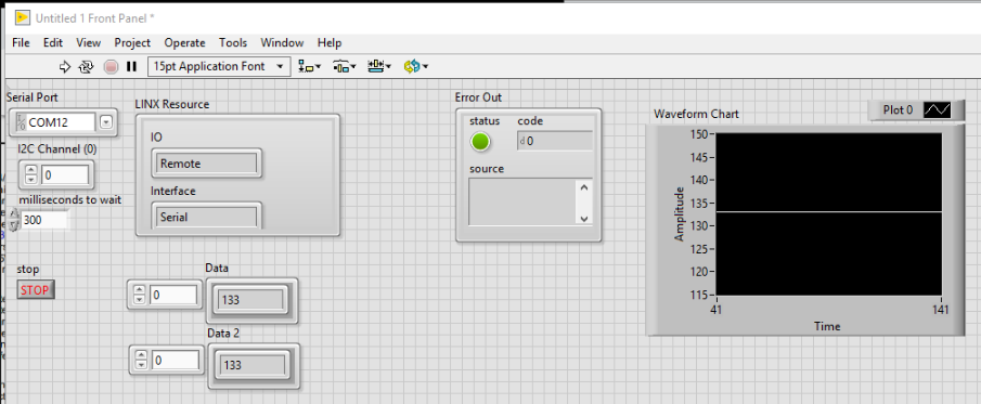
The LabVIEW (graphical) code looks like:

This program runs without errors, but the results don't make sense to me yet.  The code above starts up the i2c interface and then sends a series of i2c commands (the "quickstart" series from the datasheet, page 8, cdn-shop.adafruit.com/.../ads1015.pdf):

i2c Write 0b10010000

i2c Write 0b00000001

i2c Write 0b00000100

i2c Write 0b10000011


i2c Write 0b10010000

i2c Write 0b00000000


i2c Write 0b10010001

i2c Read 

i2c Read 

The LabVIEW program returns 133_10 from both of the i2c read commands at the end of the program sequence.

133_10=0b10000101=0x85

So, the total data returned from the ADS1015 would then be 0b1000 0101 1000 0101 = 0x8585 ?

This is the 12bit ADC, so I think (again, based on the datasheet) that the relevant part of the i2c signal is 0b1000 0101 1000 0101, ie, the ADC reading is -2^11 + 64+16+8 = -2048+88 = -1960_10 out of a possible +/- 2048?  Assuming no scaling (and the board was connected to 5v supply this would be a reading of about 5v*(1960/2048) ~= -4.78v ?

0. Should I be troubled that the "reserved" part of the returned (read) i2c signal (Conversion Register) is 0101?  What does "0h" in the spec sheet mean?  Does this part of the conversion register mean something special?  

1. Does my analysis of the ADC signal seem like a plausible result?  Am I thinking about the returned signal in the right way?  

2. In the quickstart demo, which of the four analog pins am I reading from?  Am I using amplification, single-ended vs double ended, etc?  I'm still confused about this part of the datasheet.

Grateful for any comments on what I'm doing wrong!

  • Nathan,


    When debugging digital communications, the first thing I think you should do is get an oscilloscope or an logic analyzer and look at the lines between the device and the microcontroller. For the ADS1015, I find that the best thing is to look at these lines and compare them to the communication figures shown in Figures 15 and 16 on pages 20 and 21 in the datasheet (note that there's a newer version of the datasheet on the TI website here: www.ti.com/.../ads1015.pdf ). These are going to be the best examples of how to communicate with the device.

    In your version of the datasheet, there is a difference in the MSB byte written to the configuration register. In that datasheet, the MSB byte is 0b00000001, in the newer datasheet, this is 0b10000100. In the newer version, this starts the conversion, sets PGA[2:0]=010 so that the input range is ±2.048V, and sets the device to continuous conversion mode. I would probably start with this setting, unless you need to start with a larger input range.

    Going to your questions, here are my answers:

    0. At this point, I think you have some problems with the read of the conversion. You might be reading the configuration register, not the conversion register. The default value of the configuration register is 8583h. Note that we often use the h for hex notations (0h is the same as 0x0). Also, it could be that you're reading the device but reporting back the first byte twice in the GUI. Again, you should get an oscilloscope and check the communications directly.

    1. The ADC only uses the internal reference as the reference, it never uses the supply (5V) as the reference. If you were to measure the input voltage of 5V, you would need to use the ±6.144V range. This would give a value of 1667 as a positive result, or 683h in hex.

    2. In the quickstart guide you first write to the configuration register. The first byte is the address. The second byte is 0b00000001 as the pointer to the configuration register. The third and the fourth byte are the configuration register. These are the values you want to set for the ADC. These set the gain, data rate, and all functionality. In the new version of the datasheet, Look at Figure 21 and Table 6.


    Joseph Wu