Other Parts Discussed in Thread: PCM1792A,
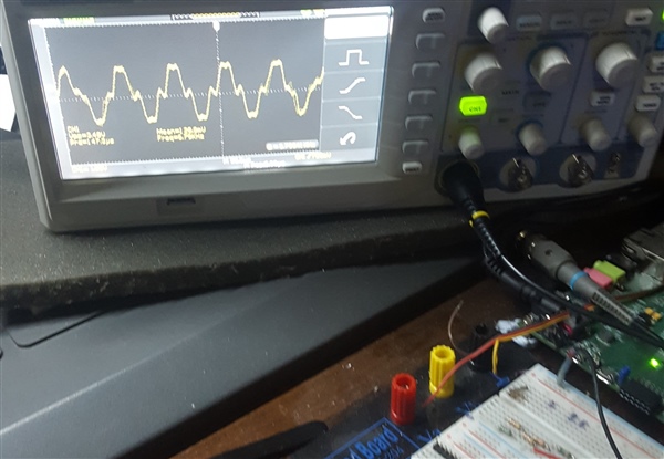
I might be doing something wrong, but I've been through all the simulations I can with my VHDL code, I know my DAC is working (PCM1792a) as I've been able to generate and output a sawtooth wave from the FPGA. When passing a sine, triangle or sawtooth wave through the PCM1802 into the FPGA and out to the PCM1792A the output signal is very noisy. It sort of improves with frequency but with glittering and undesirable noise. My clocks are fine, I am basing everything off the serial block and timing everything to that.
My ADC receiver code is below:
library IEEE;
use IEEE.STD_LOGIC_1164.ALL;
use ieee.std_logic_arith;
use ieee.std_logic_unsigned;
use ieee.numeric_std.all;


entity I2SRX is
    Port ( CLK  : in STD_LOGIC;
           CL   : IN STD_LOGIC;
           DIN  : IN STD_LOGIC;
           LD   : out STD_LOGIC_VECTOR (23 downto 0);
           RD   : out STD_LOGIC_VECTOR (23 downto 0);
           FCK  : out STD_LOGIC;
           SCK  : out STD_LOGIC;
           BCK  : out STD_LOGIC;
           LRCK : out STD_LOGIC);
end I2SRX;

architecture Behavioral of I2SRX is
signal CLKDIV : integer range 0 to 260;
signal CLKDIV2: integer range 0 to 10000 := 0;
signal CNTR   : integer range 0 to 24 := 23;
signal CNTR2   : integer range 0 to 50;
signal CNTR3   : integer range 0 to 4 := 0;
signal D1     : std_logic_vector(23 downto 0);
signal D2     : std_logic_vector(23 downto 0);
signal D1P     : std_logic_vector(23 downto 0);
signal D2P     : std_logic_vector(23 downto 0);
signal BUF     : std_logic;
signal CLK1   : std_logic := '0';
signal CLK2   : std_logic := '0';
signal FME    : std_logic := '0';
begin
--BLCK GENERATION
process(clk, CL)
begin
     if (CL'event and CL = '0') then
--        BUF <= DIN;
        if (CLKDIV2 = 1) then
            CLKDIV2 <= 0;
            CLK2 <= not CLK2;
        else
            CLKDIV2 <= CLKDIV2 +  1;
        end if;

        if (CNTR3 = 3) then

           CNTR3 <= 0;
        else
           CNTR3 <= CNTR3 +1;
        end if;
     end if;

      --BCK <= CLK2;
end process;
process(FME)
begin
    if (FME'event and FME = '0') then
        if (CLK1 = '0') then
            D1P <= D1;
        else
            D2P <= D2;
        end if;
    end if;
end process;
--LEFT RIGHT CLOCK GENERATION
process(clk,CLK2)
begin
     if (CLK2'event and CLK2 = '0') then

        if (CLKDIV = 31) then --was 31
           CLKDIV <= 0;
           CLK1   <= not CLK1;
           --LD <= D1;
           --RD <= D2;

        else
           CLKDIV <= CLKDIV +  1;
        end if;

     end if;
end process;
--process(CLK)
--begin
--    SCK <=CL;
--    if (CNTR3 = 3) then
--        BUF <= DIN;
--    end if;
--end process;
process(CLK,CLK2)
begin
    if (CLK2'event and CLK2 = '0') then
        if (CNTR <= 23) then
            if (CNTR /= 0) then
                CNTR <= CNTR - 1;

            else
                FME <= '0';

                if (CLKDIV = 0) then
                    CNTR <= 23;
                    FME <= '1';
                end if;
            end if;
        end if;
    end if;
    if (CNTR <= 23) then
       if (FME = '1') then
            if (CLK1 = '0') then
                D1(CNTR)  <= DIN;
            else
                D2(CNTR)  <= DIN;
            end if;
       end if;
    end if;
--    BCK <= CLK2;
end process;
 LD <= D1P;
 RD <= D2P;
 BUF <= DIN;
 LRCK <= CLK1;
 BCK <= CLK2;
 FCK <= FME;
end Behavioral;


