This thread has been locked.

If you have a related question, please click the "Ask a related question" button in the top right corner. The newly created question will be automatically linked to this question.

ADS1299: power down and external reference

Other Parts Discussed in Thread: ADS1299, REF5045

Hello-

This question relates to the flag PD_REFBUF/ of the ADS1299. We have several ADS1299 configured in daisy-chain mode, one chip is supposed to provide the 4.5 reference voltage to all other chips. Therefore, the reference buffers of the "slave" chips are powered down. As a result, the 4.5V drops to an arbitrary value. (we would actually expect such behavior from a powered-down operational amplifier; however, the data sheet states that a reference voltage may be applied externally, and the input impedance is 5.6k)

What else needs to be configured so that an ADS1299 accepts an external reference? In the current configuration there seems to be quite a current draw.

Thank you :)


Bernhard

  • Hey Berhard,

    By powering down the internal reference buffer, an external reference voltage may be supplied to the device. However, I would not recommend connecting the buffered internal reference of one ADS1299 to others. The internal reference buffer on the ADS1299 has limited drive strength and may not be able to effectively supply charge to other reference inputs. If you wish to use one device as a reference, I recommend buffering it with an amplifier whose bandwidth and drive strength can meet the requirements imposed by the reference inputs.

    Regards,
    Brian Pisani
  • hello Brian,


    thank you for the answer! I thought we must have a mistake, as the data sheet says "This power-down is also used to share internal references when devices are cascaded". Is the source impedance of the reference buffer really that low? The datasheet does not show drive capabilities of the source. Do you know details?

    As far as we see from measurements, reference noise seems to be negligible. So, the easiest solution could be that each chip uses its own reference. Would we miss in important aspect by doing so?

    Thank you -

    Bernhard

  • Hey Bernhard,

    The input impedance to the reference input for the device is low since, unlike the signal inputs to the device, the pin does not represent a CMOS gate (in reality, it is a switch-capacitor load). I believe one of my colleagues tested the output drive strength of the on-chip reference one time and it had under a milliamp of drive strength. I have a hard time giving you an actual limit since that was only for one chip.

    I think using the on-chip reference buffers for all of the devices is a good idea; it saves money and board space versus using an amplifier to drive all the other references. The only downside would be that all the devices would have slightly different gain error due to slight differences in the reference voltage on each device. However, the Vref accuracy is typically +/-0.02% so you'd be looking at some pretty small differences.

    Regards,
    Brian Pisani
  • Hello Brian,

    thank you for answering so quickly and sorry for still bothering you ;) We are researching this more; we notice that the prototypes that we made end of 2012 do not have the problem. The Vref buffer had no voltage drop when driving three or five parts. That was one of the reasons why we suspected an error in the circuit of the devices in production. There are no differences, and the same firmware of the controller results in the same. So, maybe it was at the edge before and a little change in the chip revision led to the situation that we have. The whole investigation started as sporadic failures of the devices were reported (thats aaargh for medical products) and the design of a device with more channels is underway. I suspect the Vref source to be the cause.

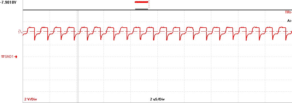
    Now, more measurements and tests make the situation weirder and weirder. We disconnected the Vref pin from the rest of the circuit to measure the current. Finding: a) the voltage is still not 4.5V but randomly slightly lower (e.g. 4.4V, and b) the current into the other chips is 0. However, when connected, we see 4.25V. I suspected oscillations of the internal buffer amp, but we didn't see anything in the first place. After disconnecting the pin, we do see a 1MHz oscillation at the pin. So, question: is this normal due to the way how the internal circuitry works and why we need bypass capacitors, or is it an unwanted oscillation of the Vref buffer? In any case, what else could be done other than having capacitors to ground? At this moment, the capacitor seems to make the oscillation only invisible, but the voltage drop suggests that it is still there.

    Now, regarding a solution, the difference of the Vref sources is no problem; We could turn on the individual Vref buffers, which does work here. However, given the problem with the oscillations I wonder if the solution could also not be sufficient.

    Looking at the solution of individual Vref sources, I wonder about the noise that Vref adds to the signal. With one source the noise would be common mode. I had the impression that its contribution is negligible. Have there been measurements, especially regarding slow drifts? Is the recommended 100uF capacitor really necessary? We did a couple of tests, and the source seems pretty stable, but I wonder if TI has more data. 

    Given the information that the internal Vref buffer's drive strength is below 1mA (we see 2mA short-circuit current ;), then a single REF5045 could then drive more than ten ADS1299  with its 10mA max output current. Maybe we just add one REF5045 part ;)

    Best,

    Bernhard

  • Hey Bernhard,

    It's no trouble at all. I confirmed silicon has not changed since the release of the device, so I doubt that the quality of shipped devices has degraded. Perhaps devices that failed were failing due to continuous use versus the prototype boards which may have been used on a more infrequent basis.

    The data that you collected in that scope plot is very indicative of how the delta-sigma modulator samples data. The frequency at which the drooping occurs happens to be the sampling frequency: 1.024 MHz. I mentioned in my previous post that the reference represents a switch capacitor load. The switch closes and opens at a rate of 1.024 MHz and needs to charge a capacitor quickly in order for there to be an accurate comparison voltage for the input. So it is not really oscillation; it is the voltage of the buffer output being pulled down due to instantaneous current draw by the reference input.

    The capacitors external to the device are required as a means to store charge that can quickly supply that instantaneous demand. The requirement of the reference buffer is then to have enough bandwidth to maintain the voltage of the external capacitor such that it is completely charged by the time the modulator samples the input. What you see in that image is that the voltage droops to the instantaneous demand and begins to start charging, but the switch opens again before the buffer has time to stabilize that voltage. The external capacitor will essentially provide charge such that the voltage there can be stabilized almost immediately.

    If you are satisfied with the quantity of noise on the internal reference specified in the datasheet knowing that the “oscillations” will disappear once the external shunt capacitors are included, then I recommend using the internal references for the individual devices. The REF5045 has a large short-circuit current, but its bandwidth is not specified. A high bandwidth amplifier is typically required to drive the reference for reasons stated above.

    TI has a lot of data regarding noise and drift of the reference. The data that is specified in the electrical characteristics table of the datasheet was determined by thorough testing of a statistically significant quantity of devices and the limits are typically guaranteed through production test. If you’d like more information regarding TI’s quality policy, refer to this link: http://focus.ti.com/quality/docs/qualityhome.tsp

    I hope this information was helpful.

    Regards,

    Brian Pisani

  • Dear Brian,

    thank you so much! This makes a whole lot of sense and I am very happy about this explanation :-)
    I was really puzzled this morning as after disconnecting the pin 24 from the rest of the circuit (i.e. two reference inputs and all the capacitors (1x 10uF and one individual 100nF) the capacitors discharged very slowly, actually as slow as I would expect to see by the multi-meter. Of course I realize that the current draw of the above mentioned mechanism is very different from a simple resistive load. In the first place the REF inputs looked like very high impedance inputs.
    I'm still puzzled why we do not see the issue in the prototypes which use the exact same circuitry. Maybe its the capacitors, but there is no ripple.
    The other item that I mentioned, the sporadic failures seem at least unrelated. These might be related to user errors ;)

    Thank you again,
    Best regards,

    Bernhard
  • Hey Bernhard,

    I'm glad to hear that you are satisfied with the explanation. I'm not totally sure what is responsible for the differing performance between devices, but I still would not recommend using one device's internal reference buffer to drive multiple devices' references. I could see a situation where the quantity of charge demanded at one particular time would be too large for one buffer to supply. Anyways, if you have any more questions, feel free to post again.

    Regards,
    Brian Pisani