This thread has been locked.

If you have a related question, please click the "Ask a related question" button in the top right corner. The newly created question will be automatically linked to this question.

DAC38J82 buswidth of SERDES and lane config

Other Parts Discussed in Thread: DAC38J84EVM, DAC38J82

Hi,

I am using the DAC3XJ8X EVM with Xilinx FPGA with FMC interface.

From DAC3XJ8X EVM GUI v1.0, there is a setting of "SERDES and Lane Configuration", there is a parameter of "Buswidth", it looks it can only  be 16 or 20bit.

but my FPGA design requires JESD204B core to have 32bit in and SERESE buswidth = 40bit, so when I look at the DAC output, it looks only half of the samples are sent out, and the other half samples can not be seen from the DAC output.


my setting is LMFKS = 4 2 1 20 1. so lane0 and 1,

lane0  <= { tp_dac_i[0][15:8], tp_dac_i[1][15:8], tp_dac_i[2][15:8], tp_dac_i[3][15:8] } ;  
lane1  <= { tp_dac_i[0][7:0],  tp_dac_i[1][7:0],  tp_dac_i[2][7:0],  tp_dac_i[3][7:0]   } ;

but from the output, it looks only tp_dac_i[0] and tp_dac_i[2] are seen.

is this related to  buswidth ?

  • Hi Weiqiang,

    The buswidth isn't the issue - remember that for each lane we're serializing the data into a single bitstream and then deserializing back to parallel data. The FPGA, with a buswidth of 40-bits, takes 40 bits (4 octets) and serializes them up to a single stream at 40 times the parallel clock rate. The DAC, with a buswidth of 20-bits, takes 20-bits at a time from the serialized stream and deserializes to a parallel clock at 1/20th the linerate. This just means that the DAC clock runs twice as fast as the FPGA clock.

    I suspect your JESD clock divider is not set correctly if you're skipping samples. This could happen if the JESD clock divider is set to double the correct value. This may be fixed by setting the JESD clock divider to half the divide ratio (e.g. if you have divide by 4 set, change to divide by 2). Please download the DAC38J84EVM GUI and use the Quick Start feature to check the rest of your settings.

    Regards,
    Matt Guibord

  • Hi, Matt

    I tried your suggestion but it is not working, but I manage to achieve the dac output rate by doubling the JESD clock at the FPGA side and change the FPGA  input from

    tx0_tdata  <= { tp_dac_i[0][15:8], tp_dac_i[1][15:8], tp_dac_i[2][15:8], tp_dac_i[3][15:8] } ;  
    tx1_tdata  <= { tp_dac_i[0][7:0],  tp_dac_i[1][7:0],  tp_dac_i[2][7:0],  tp_dac_i[3][7:0]  } ;

    to

    tx0_tdata  <= { tp_dac_i[0][15:8], tp_dac_i[0][15:8], tp_dac_i[1][15:8], tp_dac_i[1][15:8] } ;  
    tx1_tdata  <= { tp_dac_i[0][7:0],  tp_dac_i[0][7:0],  tp_dac_i[1][7:0],  tp_dac_i[1][7:0]  } ;

    e.g., increase clock twice and reduce dample rate twice, so every two sample with the same value. it looks OK from the dac output without interpolation filter, but if interpolation is applied , the wave looks not so clean.

    is this OK?

  • Hi Weiqiang,

    Please provide your required sampling rate and interpolation ratio. It sounds like there may be an issue in the FPGA JESD core configuration, however I can at least check the DAC settings against your required setup.

    Regards,
    Matt Guibord
  • Hi, Matt

    DAC38J82 baseband input fdata = 300Mhz, fdac =2.4GHz. is there anyway that I can pass your the wave form I captured?
  • Hi Weiqiang,

    Please find a configuration file attached.

    DAC38J82_300Msps_8x_421.cfg

    Regards,
    Matt Guibord

  • Hi, Matt

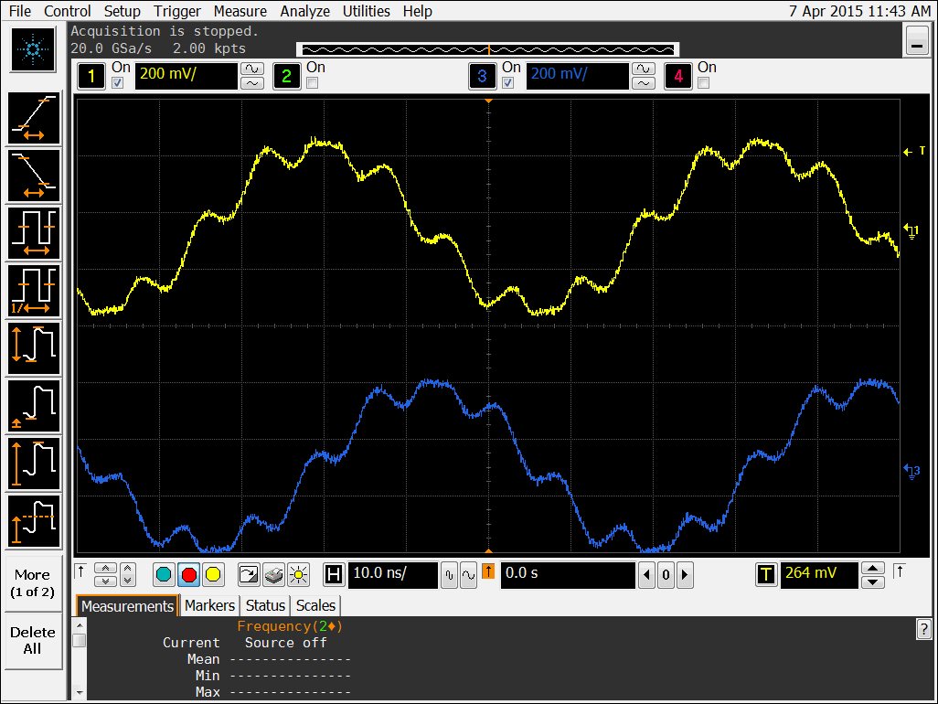
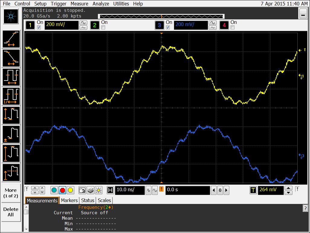
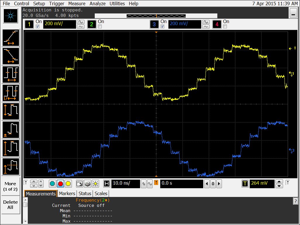
    the following is the 3 pics I captured from a scope.

    the top one is with interpolation 8,

    the middle one is with interpolation 4,

    the bottom one is no interpolation or interpolation1.

    the DAC clk =2.4G ( I replace the osc on EVM with a 100MHz part), the DAC input data rate = 300Msps. the sine waveform is generated in FPGA with T = 300M/16 = 18.75Mhz.

    so it looks the filtered signal is not so correct, is this the filter setting problem or the SERDES setting problem? I tried to attach the EVM cfg file but not sure it OK or not.

    DAC3XJ8XEVM_vco0_75m_dac2_4G_IF600m_jesd150m.cfg

  • Hi Weiqiang,

    It is not useful to look at a high speed DAC output on a scope. You're seeing the zero order hold output of the DAC. I can't say that this is not correct when it actually may be perfectly fine. You should be using a spectrum analyzer to verify that the spectrum is clean and that the DAC images are sitting at Fs+/-Fin.

    Note that you can't just change the interpolation setting on the DIG BLOCK 1 tab, since all of the clocking needs to change as well - thus the point of the quick start procedure.

    Please review some of the basic DAC concepts in the app note below to understand what you should be seeing at the DAC output.

    www.ti.com/.../slaa523a.pdf

    Regards,
    Matt Guibord
  • Hi, Matt

    as you indication,

    "Note that you can't just change the interpolation setting on the DIG BLOCK 1 tab, since all of the clocking needs to change as well - thus the point of the quick start procedure."

    so may I know how to configure these clock registers? I checked the related registers config37 and config59 and config49, any other register to check? for example, if interpolation 8x is chosen (config0 = 0x418), what is the clock to the FIR filters? how to configure?

    I think it is controlled by clock distribution circuit inside.

    best regards

    weiqiang

  • Hi Weiqiang,

    Correct, it is controlled internally by a clock distribution circuit in the chip. The internal dividers are set based on the interpolation setting, however you also need to change the serdes reference clock divider and JESD clock divider. Please use the GUI quick start tab. It will automatically calculate the DAC clock dividers based on your data rate, JESD configuration, and interpolation.

    Regards,
    Matt Guibord

  • Hi, Matt

    so may I know the relationship between "JESDCLK" and "SERDES CLK" on the "Clocking" tab of DAC3XJ8X GUI ? is Fdata = JESDCLK?  if I select the wrong clock the FIR will be wrong.

    my current target Fdata =300Msps, and I assume DACCLK = Fdac = 2.4GHz.

  • Hi Weiqiang,

    The quick start tab will automatically choose the clock dividers for you, so that you don't have to.

    The JESD clock divider is set by:

    JESDCLK_DIV = Interpolation*L/M

    L = number of lanes (1,2,4,8)

    M = number of DACs (2, 4)

    Regards,
    Matt Guibord

  • Hi, Matt


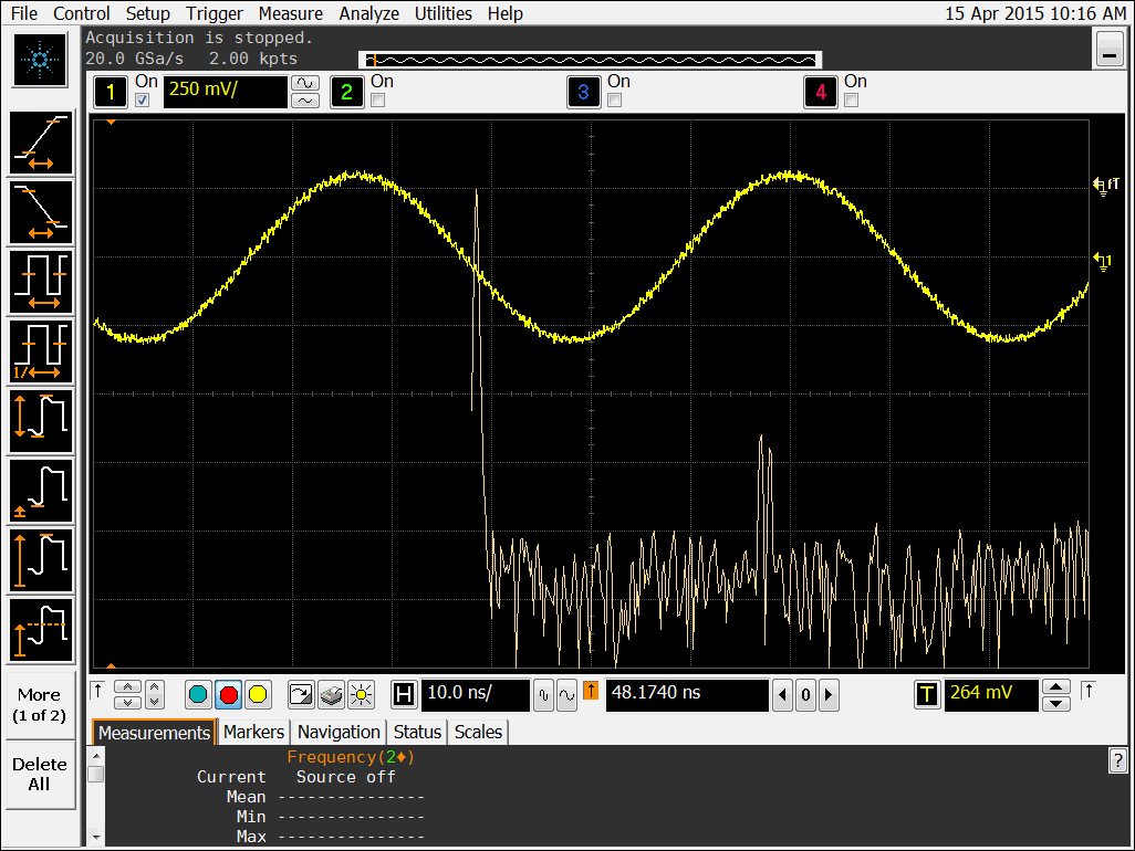
    I use the setup in slau547a (DAC3XJ8X+TSW14J56) to reproduce the issue, and it looks the same as I see in my design.

    a single freq tone  is generated by TSW14J56 EVB and sent to DAC3XJ8XEVM.

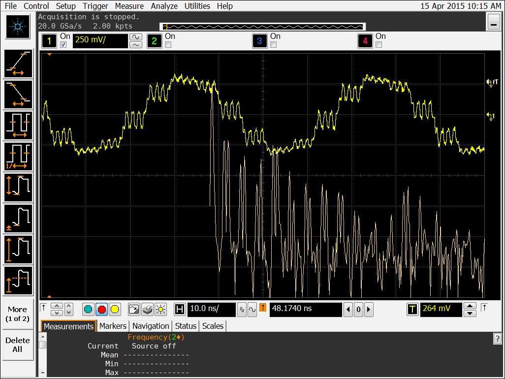
    when interpolation 4 is selected, the waveform is good,

    but if interpolation 1 is selected, there should be no interpolation and should see the DAC 16 point samples (368.64M / 23.04M), here only 8 points is shown on the scope.

    the DAC3XJ8XEVM is with the initial setting

    is this correct?

    best regards

    weiqiang

  • Weiqiang,

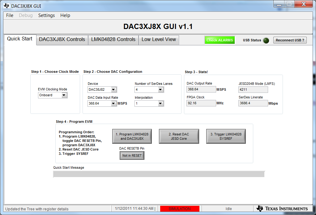
    Can you confirm that you're setting up the quick start as shown below? You should not change any other parameters in the DAC GUI.

    In HSDCPro you should select "DAC3XJ82_LMF_421" for the DAC and set the data rate to 368.64 Msps. The data format is 2's complement.

    Regards,
    Matt Guibord

  • Hi, Matt


    I think I got the idea, and my design looks OK.

    it looks that the relationship of  "DAC Output Rate" =  "DAC Data Input Rate" x "Interpolation". 

    So if "Interpolation"  is changed, the DAC clock must be changed accordingly, is this correct?


    anyway, thanks a lot.

    weiqiang

  • Hi Weiqiang,

    Correct. You'll also need to change the serdes reference divider and JESD clock dividers by the same amount.

    Regards,
    Matt Guibord