This thread has been locked.

If you have a related question, please click the "Ask a related question" button in the top right corner. The newly created question will be automatically linked to this question.

windows 7 driver for ADS5282EVM when using ADC SPI interface on PC

Other Parts Discussed in Thread: ADS5282EVM, ADS5282, ADS5281

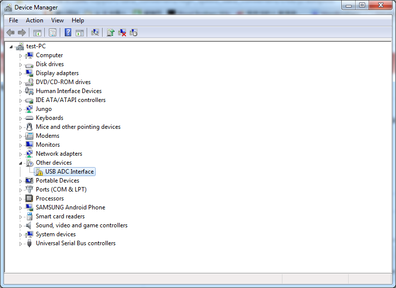
Hi, does anyone know how to use ADC SPI interface on windows 7 64 bits to initialize  the ADS5282EVM? I spend two days on how to install the driver for this evm board, searched over this website and read all post related to ADC SPI interface and adc. However, the driver for this ADC board cannot install. I also download the new driver for windows 7 from Future Technology website (because this adc board used FT245BL USB chip), but the computer cannot find any driver for this board as well. This problem is showing below.
  • Hi,

    The SPI GUI for that EVM was not updated for installation on Windows7 machines.  There are ways to make the installation work, however.  I have this GUI running on my lab PC which is Windows7.   There is a discussion of this issue in the forum posting:

    https://e2e.ti.com/support/data_converters/high_speed_data_converters/f/68/p/345453/1209238

    One of the first replies to the original post includes a document for installation instructions for Windows7 PCs.  I would re-attach that file here but at the moment the browser will not allow me to do so.  the file name is TI ADC SPI 5p2 installation for Windows 7.docx. 

    Regards,

    Richard P.

  • Hi,

    Richard, thank you very much for your help. Right now, I know how to connected ADS5282EVM to Windows 7 PC, but I cannot find the TI ADC SPI 5p2 software on any website, only TI ADC SPI 5p1 was found. Do you know where I can download this software? The ADS5282EVM I bought didn't come with any cable or CD. So, the only way I can have this software is to download from website.

    You mentioned that the FPGA may not even be toggling the high frequency for a high speed ADC such as 50MSPS. I am connecting ADS5282EVM to ML605, and I read the document XAPP1071 Connecting Virtex-6 FPGAs to ADCs with Serial LVDS Interfaces and DACs with Parallel LVDS Interfaces, it mentioned that it is OK for a Virtex-6 FPGA to connect a 12 bits, 80Mhz sample rate with 1 wired interface type ADC. Now, I feel confused about this connection, do I need to reduce the frequency of frame clock to ADC so that the FPGA can easily toggle the output bit clock of ADC?

    Regards,

    Deqi

  • Hi,

    If I remember right, in the SPI GUI version 5.1 there is a possibility that clicking one of the buttons on the panel will 'undo' an earlier clicking of a different button.   That is, if two features are each enabled by a different bit in a register such as bit0 for one feature and bit1 for the other feature - the button for one feature writes 0000 0001 to the register regardless of what the other button had already chosen.  That was fixed in 5.2.  And I believe that the bug was on the tab for the ADS5282 that you are using.  I dont have 5.1 installed on my machine anymore so I can't test it out right now.    But you can test it out by clicking on all the buttons and watching what gets written to the device by watching the ADC SPI History window in the upper right corner.  In the meantime I will try to get a drop-box set up for the installer for the SPI GUI 5.2 for you to download from.  Windows is telling me that the installer is about 100Mbyte, which seems a bit larger than it should be but too large to email anyway.

    If you wish to run the ADS5282 at 80Msps then the data rate on each serial line would be right at 960Mbps on the LVDS.  The FPGA used on our old TSW1200 capture card was Xilinx, but was Virtex4.  In that FPGA the IDDR LVDS input cell could in theory operate as fast as 1000Mbps, but in reality the input would only operate that fast if the LVDS driver that sourced the data gave enough setup adn hold time for the data bit around the DDR clock.   At 960Mbps, the bit interval for each serial bit would be about 1042ps/bit.  The FPGA requires a certain amount of setup/hold time out of that 1042ps.  The ADC skews between clock and data account for a certain amount of time taken from that 1042ps.  If the ADC doesn't give the FPFA enough of the valid data time then the actual max serial rate is lower than the theoretical max.  I dont know the timing numbers for the newer Xilinx FPGAs, but you would have to get that timing for the Virtex6, and with the timing numbers from our ADC datasheet do a static timing analysis (STA).  The Xilinx design tools have the static timing analysis tools included.  You'd have to implement a design for your ADC interface, create a timing constraint that describes the timing of the ADC, and run the STA tools. 

    There are different ways to implement the latching of the data in the FPGA and do the deserialization.  The way I did it was to use the IDDR cells to latch in the data from all eight channels plus the frame clock line, using the bit clock as the DDR clock.  The the IDELAY cells were also used to make the setup/hold timing work into the FPGA. After that it was all purely digital logic to deserialize the data using the latched frame clock.  A sketch of how that logic looked is included in this post:

    https://e2e.ti.com/support/data_converters/high_speed_data_converters/f/68/t/47555  and the link to the gif sketch is:

    https://e2e.ti.com/cfs-file/__key/telligent-evolution-components-attachments/00-68-01-00-00-16-80-49/TSW1200-Deserial.gif 

    Xilinx would be able to help with the Xilinx app notes that you find from them on the topic. 

    Regards,

    Richard P.

  • Hi Richard,

    Thank you very much for your help.

    Regards,

    Deqi

  • Hi,

    I also have same issue to connect to FPGA and reset ADC EVM.
    I have ADS5281 EVM and connected it to FPGA Virtex5 (SX95T) board.
    But I just captured DC-like signal of bit and fram clocks and data signal on chipscope (FPGA) and oscilloscope.
    Could you help me what's wrong with ADS EVM?
    And also I did reset by SPI GUI without successful driver install.
    Of course I got a error message from the GUI, but after press ok button, in the gui display I could see some signal pattern of such SCLK or CS etc.
    Do I must reset the ADC EVM before use it?
    Or can I skip the reset or any setup by SPI GUI before interfacing ADC with FPGA?
    Actually after reset by SPI GUI, I didn't get any signals from ADC and I can't see the USB connection of ADC EVM to my desktop (windows 7, 64 bit).
    Please help me to solve this problems.
    Thanks,

    Soo Mee.
  • Hi,

    the SPI GUI for this EVM was developed before there was Windows7 and the installer does not work with Windows 7.  Up at the very top of this posting there is reference to another posting that contains an instruction document on how to make the SPI GUI work on Windows 7.  I am re-attaching that document here,  please see attached.  You must get the SPI GUI working with the EVM first such that you do not get the 'bit bang' error when you click on a button such as reset.

    You should start with a reset to the ADC, and then you will want to set the clock input for differential.  I believe the default setting for the ADC after power up and reset is for single ended clock but the EVM is set up to input a differential clock to the ADC.  The clock from your signal generator is transformer coupled on the EVM and doing single ended to differential conversion so the SPI GUI should be used to select differential. 

    After that you would just need to use chipscope to debug your ADC interface as you deserialize the data lines.TI ADC SPI 5p2 installation for Windows 7 (1).docx

    Regards,
    Richard P.

    BTW, you have duplicate postings so I will delete the other posting.

  • Thanks, Richard.

    1. I'd like to do all procedure according to the document you attached, but I can't see our device, ADC EVM in device manager list.

    I powered up ADC EVM by connecting 5V supply and ground to EVM and then connect the ADC to one of usb ports on my desktop.

    But my desktop (even my labtop too) doesn't show the connection of device ADC in device manager.

    I don't know whether my ADC EVM is problematic or the usb connection part is problematic.

    Please give me some comments on how to verify where the problem takes place in our ADC EVM.

    2. According to the word document of intalling ADC device driver, after successful driver install, I should install SPI GUI software, ADC SPI 5p2.

    But I cannot search this software version on TI website. So could you send the 5p2 version? my email is smeekim@kaeri.re.kr.

    3. Could you give me verilog (or vhdl) code for interfacing ADC with FPGA?

    Regards,

    Soo Mee.