This thread has been locked.

If you have a related question, please click the "Ask a related question" button in the top right corner. The newly created question will be automatically linked to this question.

ADS54J60 / KC705 : Channel setting and Latency

Expert 8760 points
Other Parts Discussed in Thread: ADS54J60

Hi team,

My customer is going to connect ADS54J60 to KC705, and has following two questions.
Please let me know the answers. I could not find the answers in the datasheet and E2E.

(1) How can I set ADS54J60 to output through only channel B.
      KC705 connects to only channel B of ADS54J60.
 
(2) Please let me know ADS54J60 TTXLFMC value and TXOUT value.
      I need these values to calculate end-to-end latency.

    As to TTXLFMC and TXOUT, please refer to page.60 of following Xilinx LogiCORE IP Product Guide:
    www.xilinx.com/.../pg066-jesd204.pdf

 JESD Parameters are as follows:

 ・LMFS             : 4211
 ・JESD PLL Mode    : 40x
 ・f_SYSREF         : 3.125MHz
 ・k                : 32
 ・f_LMFC           : 12.5MHz
 ・Decimation filter: none

Best regards,
Fumio Nakano

  • Fumio,

    Run the ADC in a LMFS mode of 4211. The FPGA should then be set up in 2221 mode as only two lanes will be active. Then power down CHA by going to master page 080h and write the following data to the following addresses

    Address              Data

    20h                     F0h

    21h                     30h

    55h                      10h

    I am checking with the design team regarding question #2.

    Regards,

    Jim 

  • Jim-san,

    Thank you for your prompt reply.

    Regarding answer #1, please let me know the Frame Assembly.
    Is it like the following?

    DB0   A0[7:0]  A1[7:0]  A2[7:0]  A3[7:0]
    DB1   A0[15:8] A1[15:8] A2[15:8] A3[15:8]
    DB2   B0[7:0]  B1[7:0]  B2[7:0]  B3[7:0]
    DB3   B0[15:8] B1[15:8] B2[15:8] B3[15:8]

    Regarding question #2, I will wait for the answer.
    Thank you for your cooperation.

    Best regards,
    Fumio Nakano

  • Fumio,

    You will only be getting data from lanes DB1 and DB2. The data on these lanes will be as follows: 

    DB1   B0[7:0], B1[7:0], B2[7:0], B3[7:0]
    DB2   B0[15:8], B1[15:8], B2[15:8], B3[15:8]

    There will be no A data as you have shown since CHA does not have any lanes routed on the KC705.

    Regards,

    Jim

  • Jim-san,

    Thank you for your prompt reply.

    Regarding answer #1, I will tell the customer that ADS54J60 output channel can not be changed
    by setting register.

    Regarding question #2, I'm waiting for the answer.
    Thank you for your cooperation.

    Best regards,
    Fumio Nakano

  • Fumio,

    We currently do not have the numbers for question #2, and due to prioritize, we will not get around to measuring these until some time in January. Sorry for the delay.

    Regards,

    Jim

  • Jim-san,

    Thank you for your reply.

    I told the customer that US team doesn't have the numbers for question #2 and the measurement would be performed in January.

    The customer told us o.k and the customer would wait until January.

    Thank you for your cooperation.

    Best regards,
    Fumio Nakano

  • Jim-san,

    Thank you for your support.

    Please let me know the measurement schedule in January.

    Best regards,
    Fumio Nakano

  • Fumio,

    1. Does customer want to bring both channels data on channel B only? Or he wants to power down channel A and just use channel B?

      If he wants to see both channels data on channel B only, I think it may not be possible. However, he can bring both channels data to channel A’s output pins:

      If they do this the lane rate will so high that they will have to use decimation option. Device supports both channel’s data on channel A output pins with LMFS 1241 in divide by 4 option (4x decimation). See excerpt from datasheet.

    2. In which mode customer wants to know the latency? In bypass mode, the latency is 134 clock cycles as shown in timing table of datasheet. When decimation options are used, latency increases due to filtering process.

    Regards,

    Jim

  • Jim-san,

    Thank you for your reply.

    1.It seems that the customer decided to bring data on channel B only.

    2.The customer's operation mode is bellow.

     ・LMFS                        : 4211
     ・JESD PLL Mode    : 40x
     ・f_SYSREF               : 3.125MHz
     ・k                                : 32
     ・f_LMFC                    : 12.5MHz
     ・Decimation filter    : none (bypass mode)

      The latency 134 clock cycles is ADC sample to digital output latency.
      The customer wants to know the ADS54J60 TTXLFMC value and TTXOUT value.
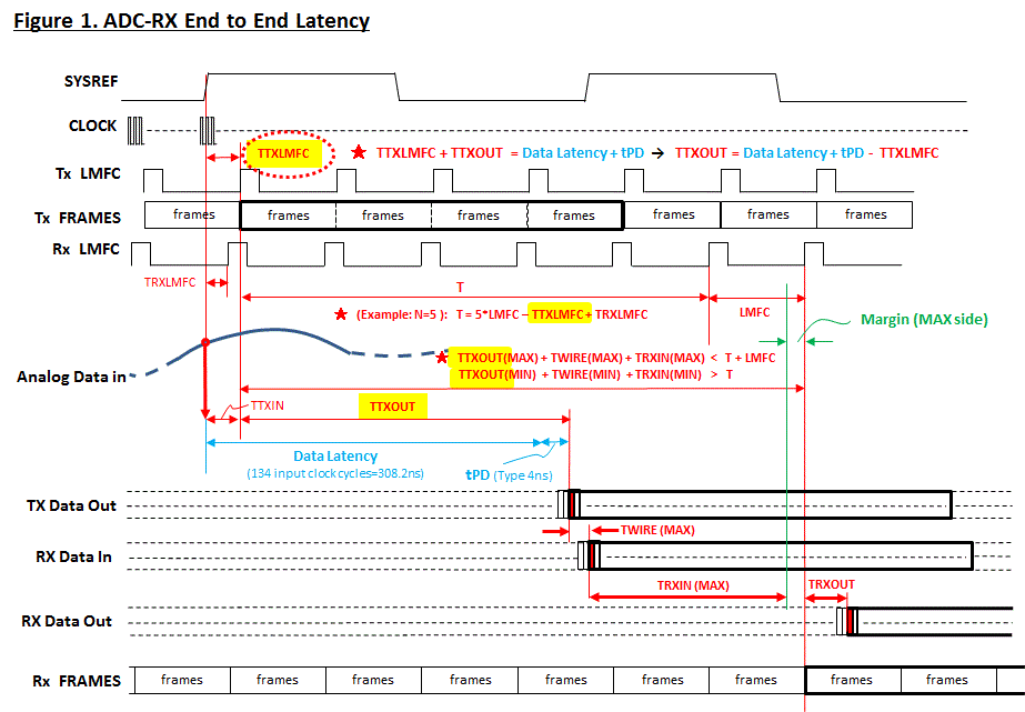
      TTXLMFC is SYSREF to LMFC latency. TTXOUT is LMFC to digital output latency.  

      Please refer to page.60 of following Xilinx LogiCORE IP Product Guide:
      www.xilinx.com/.../pg066-jesd204.pdf

      Please let me know ADS54J60 TTXLFMC value and TXOUT value.

    Best regards,
    Fumio Nakano

  • Fumio,

    So the customer will only be using CHB, correct?

    Regards,

    Jim

  • Jim-san,

    Thank you for your reply.

    >So the customer will only be using CHB, correct?

    → Yes, correct. Because CHA has no connection to KC705 on TSW14J10 board.

    By the way, please let me know ADS54J60 TTXLFMC and TTXOUT measurement schedule in January.

    Best regards,
    Fumio Nakano

  • Jim-san,

    Thank you for your cooperation.

    The customer wants to know ADS54J60 TTXLFMC and TXOUT values in order to calculate
    ADS54J60-XILINX FPGA end to end latency.

    TXOUT can be obtained from the following formula:

    TTXOUT = Data Latency + tPD - TTXLMFC ・・・(1)

    Data Latency and tPD values are listed in the ADS54J60 datasheet. So, We can know TTXOUT
    by knowing only TTXLMFC. So, please let me know ADS54J60 TTXLFMC value.

    TTXLFMC is the fixed delay from SYSREF(clocked) to LMFC. I think you can get this fixed delay
    from the design, not from measurements. So, please look into the design.

    Please refer to Xilinx LogiCORE IP Product Guide page.60:
    www.xilinx.com/.../pg066-jesd204.pdf

    And please refer to Fig 1.

    Best regards,
    Fumio Nakano

  • Fumio,
    I am still waiting on a response from the design team.
    Regards,
    Jim
  • Jim-san,

    Thank you for your cooperation.

    January will be over soon.  
    Please let me know the progress situation of the design team.

    Best regards,
    Fumio Nakano

  • F.N.,

    I have been notified by the design team that they are looking into this.

    Regards,

    Jim

  • Jim-san,

    Thank you for your quick reply.

    Best regards,
    Fumio Nakano

  • Jim-san,

    This customer needs to know TTXLMFC value by February 10th.
    Please tell this deadline to the design team.

    Thank you for your cooperation.

    Best regards,
    Fumio Nakano

  • F.N.

    I just got this from the design team. Hope it helps.

    Regards,

    Jim

    The time between SYSREF sampled by 1GHz clock (i.e. input clock) and LMFC counter getting reset can be approx. given in terms of input clock cycles with following equation:

    TTXLMFC =  4*(k+x+2)  input clock cycles.

    Where x is an uncertain number between 0 to 2.

    and k is number of frames in a multi-frame.

  • Jim-san,

    Thank you!!

    Best regards,
    Fumio Nakano