This thread has been locked.

If you have a related question, please click the "Ask a related question" button in the top right corner. The newly created question will be automatically linked to this question.

DAC8830 ATMega128 output Issue

Other Parts Discussed in Thread: DAC8830

Hello everyone,

I am currently attempting to program the DAC to work with the ATMega 128, I have a code library working and here is the basic code:

void UpdateDutyCycle(int dutyPercent)
{
//	unsigned int dutyCycle;
//	unsigned char byte0, byte1;
	/* Ensure the Clock polarity is set to FALLING */
	SPI_Set_Clock_Polarity(FALLING);

	/* Ensure the Data order is set to MSB */
	SPI_Set_Data_Order(MSB);
	
//	unsigned int test = 65535;
	DDS1_CS_HIGH; //Set the DDS CS to high
	DDS2_CS_HIGH; // Set the DDS CS to high
	VC_CS_HIGH;		// Set the voltage control DAC CS to high
	DC_CS_LOW;	// Only enable to DAC associated with the duty cycle control to low to activate it
	SPI_Transmit_Word(0b1011011011011010); // Transmit a 16-bit data
	delay_us(2); // Wait a little bit
	DC_CS_HIGH; // Set DAC CS high
}

Now for the code associated with the SPI_Transmit:

/***************************************************************
* SPI (Serial Peripheral Interface) Transmission Routine       *
*--------------------------------------------------------------*
* Transmits a single byte (or byte array) of data using the    *
* SPI bus.                                                     *
****************************************************************
* Inputs:----------------------------------------------------- *
* *cData - Pointer to the byte or byte array of data to be     *
*          transmitted.                                        *
* length - Number of bytes to transmit                         *
***************************************************************/
void SPI_Transmit(unsigned char *cData, int length)
{
	unsigned int index;

	if (length > 0)
	{
		for (index = 0; index < length; index++)
		{
			/* Start transmission */
			SPDR = *cData++;

			/* Wait for transmission complete */
			while(!(SPSR & (1<<SPIF)));
		}
	}
}

And the code for initilizing the SPI:

/***************************************************************
* SPI (Serial Peripheral Interface) Initialization Routine     *
*--------------------------------------------------------------*
* Initializes the SPI communication bus with the specified     *
* clock speed                                                  *
****************************************************************
* Inputs:----------------------------------------------------- *
* busSpeed  - Specifies the SPI bus speed (expressed as a      *
*             division of the system clock speed of 16 MHz     *
*             Values: SPI_SPR_1x2, SPI_SPR_1x4, SPI_SPR_1x8    *
*                     SPI_SPR_1x16, SPI_SPR_1x32, SPI_SPR_1x64 *
*                     SPI_SPR_1x128                            *
* dataOrder - Determines the order (LSB first or MSB first)	   *
*             that data is transferred. 					   *
*			   Values: LSB, MSB								   *
* polarity  - Determines the clock polarity setting.		   *
*			   Values: RISING, FALLING						   *
***************************************************************/
void SPI_Initialize(unsigned char busSpeed, unsigned char dataOrder, unsigned char polarity)
{
	/* Set MOSI (Master Out, Slave In) and SCK (Serial Clock) pins 
	   to outputs, leave all the other pins in their current state */
	DDRB |= (1 << MOSI) | (1 << SCK);

	/* Set the Double SPI Speed Bit */
	SPSR = (busSpeed >> 2);

	/* Set the Data order bit */
	if (dataOrder == LSB)
		SPCR |= (1 << DORD);
	else
		SPCR &= ~(1 << DORD);			

	/* Enable SPI, set mode to Master, and set the clock rate to the busSpeed */
	SPCR |= (1 << SPE) | (1 << MSTR) | (busSpeed & 0b11);
}

I should make a note that we are initializing the bus to have a prescaler of 16, on the falling edge with a data order of MSB.

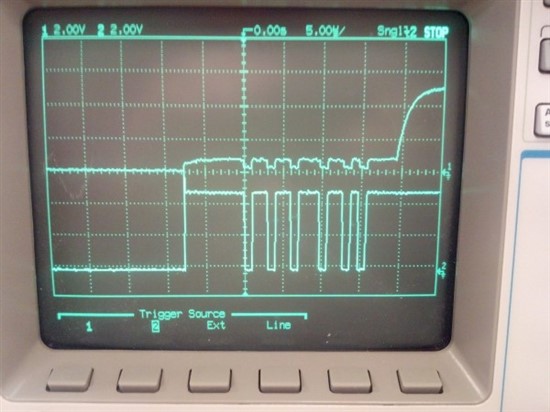
Attached is the scope shots

Figure 1


Figure 2


So Figure 1 is a scope shot of the SCLK (Scope 1) and SDI (Scope 2)


Figure 2 is a scope shot of the CS (Scope 1) and SDI (Scope 2)


My issue is this, I have a 3 Vref chip on the DAC yet, no matter what I send it, it always outputs 300 mV. I believe that it has something to do with that jitter in the CS pin. I measured the peak voltage and it came out to be 935 mV. Does anyone have any ideas?

  • Hello Phillip,


    The \CS jitter is definitely a big concern. The DAC8830 datasheet specifies the max input low voltage (VIL) as 800mV for a 5V supply.

    This means that the data being latched can be corrupted.


    Phillip Mobley1 said:
    on the falling edge with a data order of MSB

    The DAC8830 latches in data on the rising edge of SCLK. You can get some more info from page 16 in the DAC8830 datasheet.


    Also, when does \CS go low? \CS should go low before starting an SPI sequence or before the first rising edge of SCLK.

  • The CS goes low before the transmit function is executed please refer to the code up top.

    Yeah, I read the data sheet and it says this

    "Immediately following the high-to-low transition of CS, the serial input data on pin SDI is shifted out from the bus master synchronously on the falling edge of SCLK"

    I Interpreted this as setting the data out on the falling edge. And on the rising edge that is when the data is placed in the shift register of the DAC. - "latched on the rising edge of SCLK into the input shift register"

    The bus master in this case is the microcontroller. Is my Interpretation correct?

    So I am wondering, if I placed a pull down resistor, would that solve my issue?

  • Phillip Mobley1 said:
    The bus master in this case is the microcontroller.

    Correct.

    Phillip Mobley1 said:

    "Immediately following the high-to-low transition of CS, the serial input data on pin SDI is shifted out from the bus master synchronously on the falling edge of SCLK"

    I Interpreted this as setting the data out on the falling edge.

    Correct, but it is not a strict timing condition. It simply guarantees that if the data changes during the falling edge the data will be available by the rising edge for latching. 


    Currently I can see two problems:

    1. After \CS goes low. There is a rising edge on SCLK. This will latch invalid data.
      1. There are 17 rising edges after \CS.
    2. The \CS line is going above the maximum threshold for a LOW digital input.
      1. The pull-down resistor may aid the situation, but I cannot guarantee that it will solve the problem, since I have not seen this problem before.
      2. If you could share some the schematic/layout, I can check if there are any problems there.


    If you prefer to communicate privately to share your schematic/layout, is it okay to contact you to your E2E registered email?

  • Ok, so after playing around with the code, I figured out the issue

    In the microcontroller, I have to specify if the pin that I am using is either an input or an output. For this, I need it to be an output. I was accidentally setting it as an input. Once I made sure that it was being set to an output, the chip worked as it is suppose to.

    Thank you for the replies!

  • Thank you for closing the loop with the issue. This helps other people solve their problems as well.