This thread has been locked.

If you have a related question, please click the "Ask a related question" button in the top right corner. The newly created question will be automatically linked to this question.

ADS8688EVM-PDK: SPI Communication - pin ⁓RST/⁓PD - DAISY - ⁓REFSEL and others pins

Part Number: ADS8688EVM-PDK
Other Parts Discussed in Thread: ADS8688

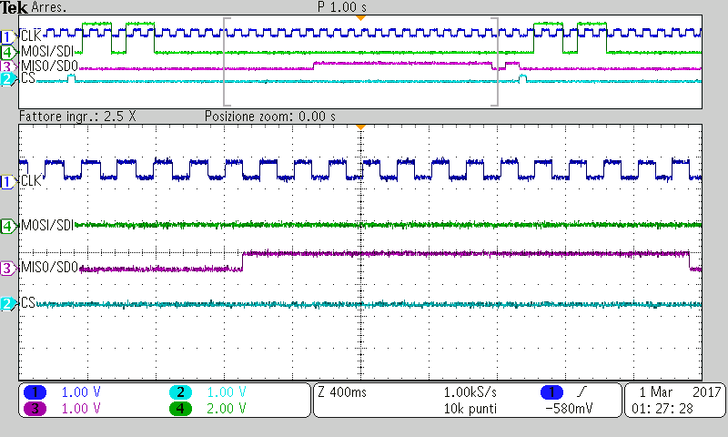
I configured my ADSEVM for a SPI communication with a host microcontroller.

In my configuration the ADSEVM is the only SLAVE of my MASTER which is the MicroControllerUnit (Arduino UNO). I want to use an internal reference.

I would like to know if I did right connection about these pins.

⁓RST/⁓PD pin

I read on the data of ADS8688 (only the ADC) that this pin can be used to set the ADS in Power Down or Reset Mode by setting it DOWN for a certain period of time. But I also saw that i can enter in this mode by using the SDI: so I decided to short it to 3.3V supply from the microcontroller(which supply the ADSEVM trough the DVDD pin). 

I "got" this signal from the connectors J1, and I would like to know which i have to do with the connectors from J3.

DAISY

As i said, I don' t have other slaves, so i shorted it to ground.

⁓REFSEL

As I said, I want to use an internal reference, so I shorted it to ground.

AGND & DGND

I suppose, looking the schematics that both of them are connected to pin GND. I shorted to ground of the microcontroller just the GND which is located up the AVDD pin.

AVDD & DVDD

I connected the AVDD to 5V and the DVDD to 3.3V supplies of MCU. Do I need to supply the ADSEVM by using other pins.

I finally use pins SDI SDO CD and SCLK as SPI Protocol request. 

I didn' t make other connections.

Notes:

I will attach a "raw" schematic to be as clear as possible. I will use your draw from the datasheet.

I was able to use the GND , AVDD, DVDD of the ADS by soldering/welding this pin to three different wires.  

  • Hello Michele,

     Most of connections you did are correct, but here are suggestions for you:

    1.  RST/PDZ pin has been pulled up to DVDD by R13 resistor on ADS8688EVM, so it’s not necessary to short to 3.3V from microcontroller again.

     2.  Daisy pin:   it’s correct to short this pin to ground if only have one ADC, but this can be done directly with J4 on ADS8688EVM.

     3.  REFSEL:  this can be shorted to ground directly with J2 on ADS8688EVM.

     4.  Power supplies:   only AVDD(+5V) and DVDD(+3.3V) are required if front-end amplifiers(U4) is not used. It’s a good practice to provide a +5V power supply to J32(Pin2) so AVDD can be created by U6 (TPS7A4901) which is a low noise low dropout linear regulator, this can create a clean AVDD supply as the ADC's analog power supply and it will be helpful to get a good performance, also +3.3V can be connected to J33.

    Please make sure that no SDCC controller board is connected when you provide external power suppliers to ADS8688EVM.

     5.  Your connections for SDI SDO /CS and SCLK are correct, all of them are necessary to activate ADC’s conversion and retrieve the data.

    Please let me know if you need more support. Thanks.

    Best regards

    Dale Li

  • Thank you so much Dale Li, I have some questions about things i didn' t understand

    AVDD Supply


    I read this on the datasheet:

    <<Do not open jumper J17 if the ADS8688EVM must be powered only from the SDCC controller card and an external 5-V supply is not provided on J32.>>

    So If I provide 5V to pin2 of J32 do I have to open J17?

    Front-end amplifiers(U4)


    When you refer to front-end amplifers(U4) do you refer to those "parts" which are connected to A0+ A1+ A2+ A3+ A4+?

    I mean, when i use AVDD and DVDD can' t I use these "parts"?

    I mean, I simply understood this:

    When I use AVDD and DVDD:

    - I can convert only signal coming from A5 A6 A7;

    - For example: If I want to convert a signal coming from A0+ I need to open J25 and close J8 between pin 2 and 3. "Basically same" for other pins;

    DAISY REFSEL & RST/PD

    Thank you i didn' t notice that the RST/PD was shorted to DVDD. But now i have a doubt, i noticed that DAISY and REFSEL are shorted by resistors R15 and R18 to DVDD too. So If i short to GND DAISY and REFSEL they are connected to DVDD too. Or am i wrong?

    USING LOGIC CONVERTERS FOR INPUT AND OUTPUT


    My MCU has digital output and input between 0 and 5V, so I need to use some 3 logic converter from 5v to 3.3V( for SCLK SDI and CD) and 1 from 3.3 to 5V(SDO). But could these produce some problem for the performance of the ADC? In reality for the moment i need only to see the ADS works :)

  • Hello Michele,

    Here are answers to your questions:

    1.  U9 is used to create high-voltage power supplies (HVDD and HVSS) with U7 and U10 together, this jumper J17 is used to enable(open jumper J17) or disable(close jumper J17 to short EN pin of U9 to ground) U9 because the function of U9's EN pin is pulling below 1.2V to disable and floating to enable this device. Because the Simple Capture Card (SDCC) is only powered by a USB port and can not support heavy loads, so this is the reason why we show the caution in page 9 to disable U9 by not opening Jumper J17 when the EVM is only powered from SDCC. If you are using external power supply on pin2 of J32, you can determine by yourself to open or close J17 which depends on whether you want to use front-end amplifiers(U4,U5) with HVDD and HVSS or not.

    2. When using AVDD and DVDD, you can convert the signals on all of input channels, including A0, A1,A2,A3, not only A5,A6,A7 channel. Channel A0,A1,A2,A3 have one more option to use front-end amplifiers(U and U5), definitely the amplifiers can be bypassed by jumper J8,J10,J9,J11.

    3. R13,R15,R18 are pull-up resistors for /RST, DAISY and /REFSEL pins, they are separated and these three pins can be controlled individually. 

    4. If voltage translators are used, please make sure all of them have same propagation delay and same timing parameters, any mismatching on timing will lead to wrong data retrieved. Actually ADS8688 supports wide DVDD range(2.7~5.25V) for different controllers, you can provide a external +5V power supply for DVDD on J33, so you do not need additional voltage translators.

    Please let me know if you need more support.

    Best regards

    Dale Li

  • Ok i get it. So, in each case i can use A0 A1 A2 A3 through front-end amplifiers, but if want to use them with HVDD and HVSS i need to open j17. In that case i have to be capable to provide at least (200mA or 500mA?) form j32. But in that case do I have to use even an external reference as the input signal is amplified? And what about DVDD in this case?

    Returning to my configuration (internal reference, only one ADC etc...) i had some troubles. I connected the channel A6 to 3.3V but I don' t see nothing coming from the MISO, only LOW signal. I don' t know if there something wrong with the code but if it is possible, could you check the connection I made are correct?

    -DAISY, grounded trough J2;

    -REFSEL, grounded trough J4;

    -RST/PD, i didn' t "get" this signal from anywhere;

    -AVDD, i provide 5V trough pin 2 of j32;

    -DVDD, I provide 5V trough pin 2 j33;

    -GND,  I shorted it to my MCU ground trough pin1 of j32;

    -A6+, I connected it to a 3.3V signal.

    I decided not to use the wires that I soldered/welded to pin GND, AVDD, DVDD.

    I didn't detach Wires soldered to these pins but I ensured that they didn' t touch anything during data capture. However I think i will detach them in case previous connection are fine.

    Moreover I decided not to use logic converters as I provide 5v to DVDD.

    I will attach another raw schematic of connections I made. I forgot to say that I have default jumper settings.

  • Hello Michele,

    The external 5-V dc supply must be capable of providing at least 500 mA of current, which is mentioned in No. 9 page of User Guide. I don't fully understand "even an external reference as the input signal is amplified", you can use internal or external voltage reference.

    I have a couple of questions for your connections and process:

    1. Have you checked if AVDD and DVDD are correct on Pin 9/30 and Pin34? Pin 2 and 3 of J13 should be shorted, they should be shorted.

    2. Have you checked if the voltage on REFIO and REFCAP are correct?

    3. Check if pin 1 and 2 of J24 has been shorted, they should be shorted.

    4. Are you sending any command to ADC? if yes,  can you please upload your screenshots for /CS, SCLK,SDI,SDO here?

    Thanks.

    Best regards

    Dale Li

  • I said that because as the input signal is amplified by buffers U4 and U5 it could exceed the internal voltage reference (4V), and the ADC would not be able to make a right conversion. Or am I wrong?

    Sorry Dale Li but I didn' t understand some things:

    1. Where can I find pins 9/30 and Pin 34? Moreover I didn' t undertand what you mean for:

    "Have you checked if AVDD and DVDD are correct on pin....".     Was you asking me if i the voltage on these pin is correct?

    2.Well, I dont' know where I can get REFCAP signal. And what voltage level do i have to expect from REFCAP and REFIO?(I suppose 4V from REFIO but i am not sure). Moreover should I have to short them(REFIO and REFCAP) to anywhere or isn' t it necessary? I ask to you this because i didn' t use them.

    sorry again Dale

    edit:

    1. sorry Dale, but when you refer to pin 9/30 and pin 34 do you refer to those of only the ADS8688 (not EVM)? If yes how could i check if AVDD and DVDD are correct on these pin? And again, what does it mean doing this thing(checking if AVDD and DVDD are correct on these pin)?

  • Hello Michele,

    This ADC(ADS8688) can support high voltage true bipolar input directly up to +/-10.24V even its voltage reference is 4.096V(whatever internal or external reference), the input range is shown in the table section 7.5 in the page 7 of datasheet.

    1.  These pins 9/30/34 are highlighted as below picture 1(red circle), which are power supply pins of ADS8688.

    2.  The REFCAP pin highlighted as below picture 1as well (blue circle), you can check the voltage on these pins or capacitors connected to these pins.

    3.  The correct voltage on REFCAP and REFIO should be 4.096V shown in page 10 of datasheet and highlighted as below picture 2. Checking these pins just make sure if the internal reference is working well.

    4.  REFIO and REFCAP pin should not be shorted, please refer to the figure 62 in datasheet, and I also copied and highlighted it as below picture 3.

    5. Please use any multimeter to check these signals, just make sure the power supply LDOs work well and the connection on power supply to ADC is good,also you are making right jumper. 

    6. Are you sending any software command to ADC by SDI? this is very important. if yes,  can you please upload your screenshots for /CS, SCLK,SDI,SDO here? 

    Thanks.

    Best regards

    Dale Li

    Picture 1: 

    Picture 2: 

    Picture 3: 

  • Thank you Dale Li

    2. This is my first time I work with these parts, so I didn' t think I could do it(not sure if I could make damages). Yes i will use a multimeter;

    4. Sorry Dale, but the picture you send is for using an External Reference? I want to use an internal reference. However you right as with an internal reference they "contain" an output signal;

    6. Below the code

  • //include SPI library
    #include<SPI.h> 
    //Slave Select Pin. I will set it LOW to start communication and set HIGH to end it.
    const int ss_pin=10;  // contain the pin number of Arduino
    byte address_1; //First 8MSBit of address of channel
    byte address_2; //Last 8LSBit of address of channel
    byte voltage[2]; //It will contain the 16bit coming from the SDO of ADC
    //it is a contator to count how many measuremnt I did.
    int c=0;
    
    
    void setup() // this code will run a time
    {
      Serial.begin(9600);//settings for serial communication with PC
      pinMode(ss_pin,OUTPUT); //setting pin ss_pin as output. I need to set as output only it
      digitalWrite(ss_pin,HIGH); //Send an High signal to ss_pin
      
      Serial.println("Begin for 4 seconds"); //print message
      delay(4000);//wait 4 seconds
    
      //This Arduino has a 16Mhz frequency
      //setting for SPI Communication between Arduino and ADS
      SPI.beginTransaction(SPISettings(16000000, MSBFIRST, SPI_MODE1));
      address_1=B11011000;  //I want to use MAN_MODE by selecting channel A6
      address_2=B00000000;  //so i will set the bit from the most significant
      
      digitalWrite(ss_pin, LOW); //Set the slave select pin LOW. Start Communication
      delayMicroseconds(2);//wait 2 microseconds
      //I transfer 16 bit rapresenting the channel
      //SPI.transfer transfer 8 bit trough the SDI and return 8 bit from the SDO during only 8 clock cycles
      SPI.transfer(address_1); //first 8 bit
      SPI.transfer(address_2); //last 8 bit
      delayMicroseconds(2);
      voltage[0]=SPI.transfer(0); // I will get the first 8 bit from SDO
      voltage[1]=SPI.transfer(0); // I will get the last 8 bit
      delayMicroseconds(2);
      digitalWrite(ss_pin,HIGH);  //Set the slave select pin HIGH. End Communication
      
    }
    
    void loop() //This code will run more than one time
    {
    
      //Same
      digitalWrite(ss_pin, LOW);
      delayMicroseconds(2);
      //By sending all 0 to SDI i decide to continue make measuramente on same channel(A6)
      SPI.transfer(0); 
      SPI.transfer(0);
      delayMicroseconds(2);
      voltage[0]=SPI.transfer(0);
      voltage[1]=SPI.transfer(0);
      delayMicroseconds(2);
      digitalWrite(ss_pin,HIGH);
    
      
      Serial.println();
      Serial.println(voltage[0]);
      Serial.println(voltage[1]);
      while (c>100) // For the moment i want to make only 100 
      {
        Serial.println("END");
        delay(1000);
      }
      c=c+1;
      delay(1000);
    }
    

  • Hi Michele,
    I understand, actually the first picture is showed ADS8688 with internal reference which comes from ADS8688EVM and you are using. The 3rd clear picture is showed with the external reference from the datasheet but I only want you to see the relationship between REFIO pin and REFCAP pin because you want to short both of these two pins, the datasheet never suggest to do that.
    I would like to see a timing, can you please upload your screenshots for /CS, SCLK,SDI,SDO here? What's your CPOL and CPHA you configured for SPI interface. Thanks.

    Best regards
    Dale Li
  • Ok I didn' t understand, so do you want to see bits coming out/in from /CS SCLK SDI and SDO?. Do I have to use an oscilloscpe?

    I configured my SPI communicatin by setting CPOL =0 CPHA=1. I did this by sending the parameter SPIMODE1 to the object :

    SPISettings(frequency,MSBFIRST/LSBFIRST,SPIMODE0/1/2/3) 

  • Hi Michele,

    Yes, please use an oscilloscope to capture the signals, I want to check your timing like the below picture, and an additional zoom-in screenshot should be better if you can provide, so the detailed timing parameters can be checked as well like the table in page 11 of datasheet. Thanks.

    Best regards

    Dale Li

  • Hello Dale Li,

    I checked all the pin and results were these:

    REFIN:

    Capacitor C7 ---> 4 V

    REFCAP:

    Capacitors C8 C9 ---->4V

    AVDD

    Capacitors C63 C10 ---> 5V

    DVDD

    Capacitors C5 ---> 5V

    So as expected.

    Then I used the oscilloscope I will attach some screen refering of different situation on channel A6:

    First command and response(I receive all ones indipendently of situation on A6):

    A6+ shorted with A6-

    Connected 3.3 V to A6+ and shorted A6- to GND (even it isn' t necessary)

    Nothing connected to A6+ and A6-

    PS:

    - After using a oscilloscope I see that with the libraries nothing came out from the MCU, so I modified the code, and I decided not to use any libraries. Moreover I decided to keep the SCLK HIGH and DOWN for several time to see better what was happening. 

    - Are this consistent data? Is it normal that when I short A6+ to A6-( so to the ground) I received all 1. I have a doubt. At 16th falling edge of CLK the first significant bit come out from MISO(SDO)? I read something like this on datasheets but i m not sure.

    -What is strange is that SCLK CS and MISO were 1V signal. But the ADC received all command, or at least i suppose it

  • Hello Michele,

    ADS8688 reads the data on the SDI line at every falling edge of the SCLK, also the output data stream is clocked out on SDO on the SCLK's falling edge. If your CPHA is configured correctly as 1, the data should be captured on the second edge(falling edge) and the data should be updated on the first edge(rising) on SDI, but your timing shows different behavior which is highlighted as below 1st picture, the correct timing is shown in 2nd picture (ADS8688's timing from datasheet). You get the data in few screenshots but they probably are not correct or you will not be able to capture correctly.Please check your controller and configuration, also please make sure your controller can read out the data during tHT_CKDO in ADS8688's timing diagram. Please let me know your result. Thanks.

    AINx_GND pins on ADS8688 should be connected to the ground directly or by a balanced resistor shown in Figure 52 of datasheet, it's necessary.

    The MSB of the output data stream is clocked out on SDO on the 16th SCLK falling edge, followed by the subsequent data bits on every falling edge thereafter.

    Your ADC's internal reference works well and the power supplies are good.

    Best regards

    Dale Li

  • Hello Dale,

    thank you for response, but I didn' understand some things:

    1) What do you mean for "clocked out"? Does the data remain on SDO between two falling edge of SCLK?

    2)I send data to SDI on the second edge of SCLK. I attached a screenshoot of this.

  • Hello Michele,

    At CPOL=0, for CPHA=1, data are captured on the clock's falling edge and data is output on a rising edge, when the controller is capturing the data n SDO of ADC or ADC is capturing the data on SDI, both of them hope to have a stable data status and the data should be kept for some time which will be easy and helpful for the controller and ADC to capture. Your timing is different and the data is changing at falling edge and stable for rising edge and it' will be critical to be captured properly. The correct timing is highlighted as below from ADS8688's datasheet:

    There is one useful web link about the SPI timing is:

    en.wikipedia.org/.../Serial_Peripheral_Interface_Bus

    Best regards

    Dale Li

  • Hello Dale Li,

    I decided to use a better MCU like MyRio in order to use a SPI library.

    1)I made different measurement from 0 to 5V and considering that the default range is +- 10V, I received consistent data. The problem is that output is availble on falling edge even if I configured the SPI well. I set the Clock Phase to Leading and Clock Polarity to High.

    2) The default voltage range is +-10V but I read that i can change it, by changing values in program register(by sending a proper sequence to ADC). I tried to send data, to change the range to 0 to 5V, but I didn' t manage it. If I want to change the range to 0 to 5V which sequence should I send to ADC? I sent to the ADC the sequence 10100001 00000110 but what I received was 10100111. Is the sequence i sent correct? I suppose not. Could you help me?

    Thank you Dale Li.

    Regards,

    Michele Fragasso

    PS:

    1)I use a 4V voltage reference;

    2)I use the A0 input channel;

  • Hello Dale Li,

    I solved my troubles

    2) What i mess is that I send the sequence 1010000 1 00000110 instead of 0000101 1 00000110. Moreover at start of communication I reset all program registers. What i received was the 8 bit sequence 00000110 so as expected this time. Moreover even the bits from A0 channel were consistent.
    1) I set the Clock Polarity to LOW and Clock Phase to Trealing when I send data to ADC, and Clock Polarity to LOW and Clock Phase to Leading when I received data from ADC, but nothing changed on output edge. However I can receive correct data from ADC.
  • Hello Michele,
    Thanks for sharing this good news, sorry for late response and I just came back.

    Best regards
    Dale
  • Thank you very much Dale Li.

    Best Regards,
    Michele