This thread has been locked.

If you have a related question, please click the "Ask a related question" button in the top right corner. The newly created question will be automatically linked to this question.

TINA/Spice/TLC2262: Some questions about TINA simulation in transient analysis and AC analysis

Part Number: TLC2262
Other Parts Discussed in Thread: TINA-TI, , ADS7046

Tool/software: TINA-TI or Spice Models

Hi,

I am now using TINA to simulate the behavior of an op amp TLC2262. But the result of AC analysis and transient analysis is different.

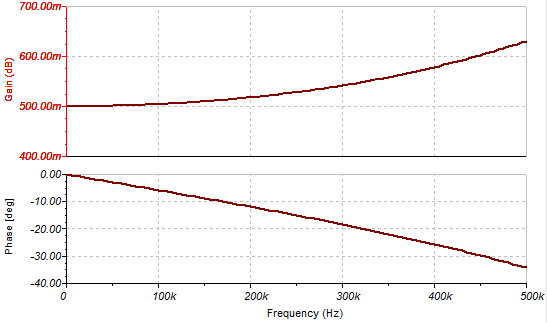
1, In the first case, it is ac analysis which operates between 1 to 500kHz and from the result below, the amplitude of the output waveform is increasing with the frequency.

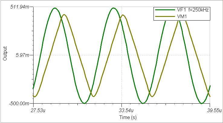
2, But when it comes to transient analysis with a 1V input at 500kHz, the amplitude is about 200mV which is a conflict with the result of ac analysis who has 650mV at 500kHz.

And here is the result of the second case:

 4604.TLC2262.TSC

Could anyone explain to me why the result behaves like this?

Thank you!

Best regards,

Haoyang

  • Hello Haoyang,

    The current op amp configuration (Vin=500mV and f=500kHz) is operated above its slew rate limit. So I think this is the reason behind the transient behavior of the model.

    The slew rate value of the op amp TLC2262 is 0.5 V/us.

    SLEW RATE= 2 * PI * f * V.

    Where

         f = the highest signal frequency, Hz

         V = the maximum peak voltage of the signal.

    For the current model, depending upon the slew rate limit, the highest signal frequency would be approx. 160kHz.

    • As an example, take the scenario where an op amp is configured with a signal with a peak amplitude of 500m volts at a frequency of 250kHz

    As can be seen in the diagram, in the limit, the op amp slewing distortion will result in the creation of a triangular waveform. If the frequency is increased further the op amp will be even less able to keep up and therefore the amplitude of the output waveform will decrease.

    Regards,

    Aditya C

  • Hi Aditya,

    Thank you for solving this problem! And may I ask you another question regarding ADS7046? I am connecting an ADC  'ADS7046' behind this op-amp.

    1, As you can see, the input sinusoidal voltage range is from -0.5 to 0.5V, but the Unipolar Input Range: 0 V to AVDD of this ADC is from 0V to AVDD according to the datasheet. Is that mean I can not use this sinusoidal input voltage from -0.5V and the AVDD should be larger than 0.5?

    2, When I changing the amplitude of AVDD, I found that the sampling time length is decreasing when AVDD is increasing. Could you please tell me the reason?

    3, The sampling rate of ADS7046 is 3M on the datasheet. But when I increase the frequency of CSV to 5MHz and SCLK to 90MHz, this ADC is still working, how could it handle a sampling frequency higher than 3MHz?

    Thank you!

    Best regards,

    Haoyang

    ADC7046 revised - autosave 17-12-30 14_36.TSC

  • Hi Haoyang,

    Please find the answers below,

    1. As per datasheet, the ADC is unipolar, so it can convert A-to-D (i.e. give digital bits) for voltages > 0 to Avdd.

    But, the ADS7046 model captures the SHA circuitry, and gives out the sampled value as the output.

    As I can see from simulation no clamping for <0V is implemented in the SHA model output, so it can sample values <0V in the input correctly, as well. So sampled output will also be seen correct.

    But the real ADC will not give correct output bits for -0.5V.

    2. Avdd should be always connected to 3.3V as per datasheet for typical operation.

    From the simulation it seems that some clamping logic has been implemented on the positive ceiling of sampled output, depending on Avdd input voltage such that, it can reach a max of, ( Avdd- some headroom value)

    That is the reason I think you could see sampling time getting elongated when Avdd and input voltage value is set nearby, because some other circuit is trying to limit the output at that time.

    3.On the sampling frequency front, the effect will be seen via settling time/ setting voltage error value.

    The spec of maximum frequency is derived from the settling time of the sampling cap needed.

    The bandwidth of the switch in Typical condition is designed accordingly (with some 20-30%  margin, ie if requirement is 3MHz, say it will be designed for %MHz in Typical)such that it meets the settling time across corner.

    Also in real design the resistance is a MOSFET so its parameters varies as with Vin, but in model we ususally have a fixed typical resistance and cap value.

    So this will serve correctly in model, even for some higher frequency than 3MHZ. After that with eventual increase of frequency, we will see that the sampling cap will be unable to track and settle so fast, so there will be more error in the sampled voltage value; or in other words it will not be able to settle to the desired value in that time frame.

  • Please read %MHz as 5 MHz