This thread has been locked.

If you have a related question, please click the "Ask a related question" button in the top right corner. The newly created question will be automatically linked to this question.

C6678 EMIF interface throughput issue

Other Parts Discussed in Thread: TMS320C6678

Hi All  ,

In our custom design we have interfaced TMS320C6678 DSP to an FPGA on EMIF16 interface.  We intend to use the EMIF for accessing the FIFO memory on FPGA for transferring data to and from FPGA. EMIIF16 is running at 166 MHz clock. The EMIF 16 timings programmed on the DSP are mentioned below :

1) Write setup : 2 cycles - 12 ns

2) Write strobe: 4 cycles -24 ns

3) Write hold : 1 cycle - 6 ns

4) ReadSetup :2 cycles - 12 ns 

5) ReadStrobe  8 cycles : 48 ns 

6) Read hold : 1 cycle : 6ns
7) Turn around time : 2 cycles - 12ns

Extended wait is disabled.

With the above mentioned settings we ran a throughput test to estimate the data rate we are able to achieve on the EMIF bus. The test is a non-BIOS project that continuously does an EMIF write to the FPGA FIFO register in a loop. The test shows a data rate of 98 Mbps for the transfer. According to the timings that we have programmed for the write we should be getting a theoretical throughput of 16 bits /( write setup +write hold + write stobe)  ~ 350 Mbps. We understand that the throughput can be lesser than the theoritical max due to code overhead but what we are seeing is more than 50% loss. We probed the signals on the EMIF bus and observed that there was a 24 cycle delay seen in the waveforms between two writes ! We are unable to find the cause of this huge delay . Does anyone have an idea where this delay could be ccoming from ? I am attaching the code which does the EMIF configuration for your reference.

   /*  FOR CHIP SELECT 0  */
      hEmif16Cfg->A0CR = (0                                         \
          | (1 << 31)     /* selectStrobe */ \
          | (0 << 30)     /* extWait */ \
          | (1 << 26)     /* writeSetup  12 ns */ \
          | (3 << 20)     /* writeStrobe 24 ns */ \
          | (0 << 17)     /* writeHold    6 ns */ \
          | (1 << 13)     /* readSetup   12 ns */ \
          | (7 << 7)      /* readStrobe  48 ns */ \
          | (0 << 4)      /* readHold     6 ns */ \
          | (1 << 2)      /* turnAround  12 ns */ \
          | (1 << 0));    /* asyncSize   16-bit bus */ \

   /* Set the wait polarity */
      CSL_FINS(hEmif16Cfg->AWCCR, EMIF16_AWCCR_WP0, CSL_EMIF16_AWCCR_WP0_WAITLOW);
      CSL_FINS(hEmif16Cfg->AWCCR, EMIF16_AWCCR_CE0WAIT, CSL_EMIF16_AWCCR_CE0WAIT_WAIT0);
      hEmif16Cfg->AWCCR = (0x80            /* max extended wait cycle */ \
        | (0 << 16)     /* CE0 uses WAIT0 */    \
        | (0 << 28));  /* WAIT0 polarity low */ \


     -Anil

  • We also used a C6678 EMIF-16 interface to an FPGA on a recent project, and I also found that I could not explain the gaps between writes in terms of what the EMIF-16 manual was telling me.  The actual strobe timings within a read or write seemed be behave perfectly fine.

    I'm not sure I ever timed it with a Release build, and I know there can be a really substantial difference in the speed of tight loops in Debug.  We had intermittent reliability issues with the EMIF Write (almost certainly the fault of the custom FPGA, not the DSP) and speed wasn't a huge issue so I gave up on tightening the read and write timings on that project.

    That said, 24 EMIF bus cycles is an age in core time (I assume you mean 24 * 133 Mhz EMIF clocks - I remember it as being around a dozen cycles, but I'd have to look back to see) and it does have a big impact on throughput...

    Gordon

  • I'm not sure exactly where the overhead is coming from.  Have you tried using EDMA for the transfers?

    -Chad

  • Hi Chad ,

    Yes . We have tried using EDMA but the reseults are same and we still see the delay between writes.

    -Anil


  • Thanks, I've asked one of my EMIF experts to take a look at this thread.

    -Chad

  • Anil,


    Hi, how many cycles does one write to the FIFO take and what was ther frequency of SYSCLK7.

    Thanks,

    joe


  • Hi Joe,

    The EMIF write timings(setup ,hold,strobe) seem to match with what we have programmed. The write takes around 6 cycles . However between two writes we observe a delay of around 24 cycles. EMIF is running at 166MHz. So here 24 cycles implies 24 EMIF cylcles.

    The extra delay is also observed between read-write and read-read transactions.

    -Anil


  • Hello,

    An additional detail for the issue we are seeing is that two successive writes appear to pipeline, and do not suffer the ~24 cycle inter-transaction delay.  The third write will suffer the delay though, and the fourth will be similarly pipelined.  So for a write only test, writes occur in groups of two, separated by ~24 cycles of delay.  We had justified this by the description in the EMIF document for turnaround time:

    Turnaround - Cycles between the end of one asynchronous memory access and
    the start of another asynchronous memory access minus one cycle. This delay is
    not incurred between a read followed by read or a write followed by a write to
    same chip select.

    However, it seemed worth mentioning as well.  Re-reading the turnaround description, it doesn't seem to apply to the ~24 cycle delay we are seeing.  It appears to occur after every read, and every other write.

    Thanks,
    Dan

  • Hi,

    How are you measuring the throughput? Do you measure the start-stop time stamps in software or are you looking at the scope shots to find out the start-stop times of the transfer? If it is measured in software, can you provide the code you used to calculate the throughput (both EDMA and non-EDMA if you have both) and also the scope shots that show the 24-cycle delay?

  • Hi,

    In our design we also have a FPGA interfaced with a C6678 through EMIF16, and have observed exactly the same behavior. 

    When we added a mfence instruction immediately after the EMIF16 write we could observe that the DSP CPU core would stall for a period significantly longer than just the EMIF16 access. This was tested by using one of the external GPIO pins on the DSP as a triggering point for the scope connected to the EMIF16 bus lines, and toggling this GPIO pin before and after a EMIF16 write access. 

    One observation made during these tests is that larger writes (32b/64b) towards the EMIF16 would be split up into smaller 16bits transactions with no significant wait periods between them on the EMIF16 bus. However, the DSP CPU core would not start executing until long after the last 16 transaction completed on the external bus.

     - 

    Kjetil 


  • Aditya said:

    Hi,

    How are you measuring the throughput? Do you measure the start-stop time stamps in software or are you looking at the scope shots to find out the start-stop times of the transfer? If it is measured in software, can you provide the code you used to calculate the throughput (both EDMA and non-EDMA if you have both) and also the scope shots that show the 24-cycle delay?

    Our throughput measurement comes from generating packets from a very simple DSP software application.  Those packets are received by an external piece of hardware that receives the signal (MPEG2-TS), and displays some statistics -- including the average stream bit rate.

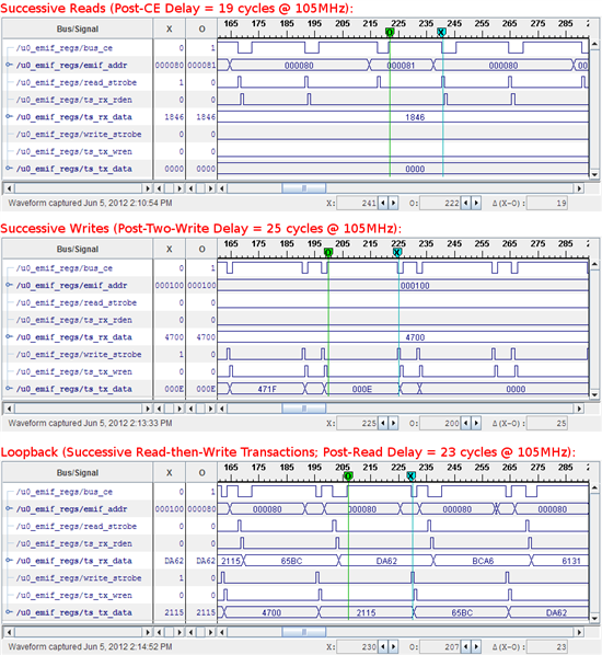
    Then, to understand the details about why we were seeing throughput much lower than we anticipated, we examined the bus using an integrated logic analyzer in the FPGA.  The signals we examined are sampled at 105MHz, and are shown in the screenshot.  First is a test using continuous reads.  It shows a delay of 19 cycles after each read.  Next is a test using continuous writes, which seems to pipeline two writes without a significant delay as I mentioned.  But the second write includes a 25 cycle delay.  Finally, a loopback test that involves reading a value and writing it back.  This demonstrates a delay of 23 cycles after a read, but no significant delay after a write.

    The various delays (19, 25, and 23 cycles) are the thing we can't quite explain by reading any of the corresponding material about the EMIF bus.

    Thanks,
    Dan

  • Kjetil Oftedal said:

    One observation made during these tests is that larger writes (32b/64b) towards the EMIF16 would be split up into smaller 16bits transactions with no significant wait periods between them on the EMIF16 bus. However, the DSP CPU core would not start executing until long after the last 16 transaction completed on the external bus.

    Hi Kjetil,

    Did the larger (32- or 64-bit) writes allow you to get more effective bandwidth, or was the delay proportionally longer?  I tried simply using a larger pointer (uint32_t) but observed the data being truncated instead of multiple transactions.  How did you set the EMIF peripheral up to handle larger than 16-bit writes?

    Thanks,
    Dan

  • Hi,

    There is a 184ns delay between each block of  4x16-bit transactions, so around 30-31 cycles on the EMIF16 clock. I did not setup the EMIF16 module in any particular way to achieve this. I only used an aligned 64-bit volatile pointer:

    volatile uint64_t* ptr = 0x70000000; /* EMIF16 CS 0 */

    *(ptr) = <some 64-bit variable> 

    -

    Kjetil 


  • Dan, Kjeitl,

    Thanks for your feedback. I am looking into this.


    Dan, are you using an mfence following the last EMIF16 access as well?

  • maril,

    You mentioned that you saw the delays when using EDMA as well. Do you or Dan have scope shots using EDMA to compare against the CPU read/write scopeshots? I would like to see part of a single EDMA burst as well as a screenshot showing the delay between two different EDMA bursts.

  • Dan,

    Hi, wouldn't you agree that the EMIF16 is really ment for NAND and NOR flash not FPGAs? If you read the datasheet it says "external memories such as NAND and NOR Flash". After reading the replies on this topic I'm beginning to believe that your best way to interface with an FPGA is something other than the EMIF.  Any comments?

    Thanks,

    joe

  • Kjetil Oftedal said:

    volatile uint64_t* ptr = 0x70000000; /* EMIF16 CS 0 */

    I did finally get this to work, for the most part.  The 64-bit write to 0x70000000 generated 4 transactions to consecutive address (0x0000, 0x0001, 0x0002, 0x0003).  The transactions were nice and close together (3-4 cycles @ 105MHz) with groups of 4 transactions separated by the "long" delay of 24 cycles @ 105MHz.

     In the image, the first write_strobe is a register access for comparison.  The following 4 write_strobe signals are the uint64_t being written out (note the emif_addr incrementing).  There is only one ts_tx_wren here because address 0x100 is the only one connected to the ts_tx_data FIFO.

    Aditya said:

    Dan, are you using an mfence following the last EMIF16 access as well?

    No.  It seems self-restricting so I didn't see the need.  Should I try that as a test as well?

    Aditya said:

    You mentioned that you saw the delays when using EDMA as well. Do you or Dan have scope shots using EDMA to compare against the CPU read/write scopeshots? I would like to see part of a single EDMA burst as well as a screenshot showing the delay between two different EDMA bursts.

    I was unable to reproduce today the exact result from our original testing with the EDMA test project we have.  However, the scope capture looked identical to that of a simple, procedural write.  Two writes were "pipelined" followed by the long, unexplained delay.  We have adjusted some timings, so that original capture is not exactly relevant today.

    After today's testing, I am at a loss as to why writing out a 64-bit value, to successive addresses, allows faster EMIF bus access than simple, unrolled 16-bit "bus word" access.

  • Dan Christensen said:

    After today's testing, I am at a loss as to why writing out a 64-bit value, to successive addresses, allows faster EMIF bus access than simple, unrolled 16-bit "bus word" access.

    I realize I didn't explicitly ask, so is there any explanation for this?  Or anything we can do to work around it, aside from changing how we access the bus?

    Thanks,
    Dan

  • joe lindula said:

    Dan,

    Hi, wouldn't you agree that the EMIF16 is really ment for NAND and NOR flash not FPGAs? If you read the datasheet it says "external memories such as NAND and NOR Flash". After reading the replies on this topic I'm beginning to believe that your best way to interface with an FPGA is something other than the EMIF.  Any comments?

    Thanks,

    joe

    Hi Joe,

    EMIF also supports ASRAM, so I think that it can be used to interface with an FPGA.

    Dan,

    Am I right to assume that the emif_addres is set in your code like(http://e2e.ti.com/support/dsp/c6000_multi-core_dsps/f/639/t/152723.aspx)

    for(i=0;i<=15;i++)
        { *(volatile  *) (0x74000000+0x4*i) = (uint32_t)(i+1);}

    Then the EMIF controller splits the 32 bit address into 4 8 bit address, right? But the emif_data remains constant during these four address changes, is that correct?

    Thanks

  • Johannes said:

    Dan,

    Am I right to assume that the emif_addres is set in your code like(http://e2e.ti.com/support/dsp/c6000_multi-core_dsps/f/639/t/152723.aspx)

    1
    2
    for(i=0;i<=15;i++)
        { *(volatile  *) (0x74000000+0x4*i) = (uint32_t)(i+1);}

    Then the EMIF controller splits the 32 bit address into 4 8 bit address, right? But the emif_data remains constant during these four address changes, is that correct?

    This is what I had for code in the above capture:

    while(1)
    {
       *(uint16_t *)0x70000000 = 0xCAFE;
       *(uint64_t *)0x70000200 = (uint64_t)0x0102030405060708;
    }

    The 0xCAFE was the uint16_t register write while the 4 writes in "rapid sequence" were the uint64_t.  The EMIF controller handled the single 16-bit write normally, and then split the 64-bit write into 4 16-bit transactions.  The four 16-bit transactions were to the following address (not clearly shown in the capture as I was missing the LSB on the emif_addr signal):  0x70000200 (data=0x0708), 0x70000202 (data=0x0506), 0x70000204 (data=0x0304), 0x70000208 (data=0x0102).  The data ordering with the incrementing address makes sense because we are in little endian mode.

    Hopefully that makes things more clear.

    Thanks,
    Dan

  • From the context, it appears Anil (maril) and Dan are working on the same project that is the original subject of this thread, and other good questions and advice have come in from Gordon, Joe, Kjetil, and Johannes, and of course Aditya. Is this correct?

    While we try to track down the real reason for this long delay between EMIF16 operations, I would like to suggest another possible way to speed up more of the process with the EDMA.

    Anil, Dan,

    Since it appears that the multi-half-word accesses (32b and 64b) are working better, this implies that when an internal bus command reaches the EMIF16 peripheral, it will be sent as a single entity and will not have the ~25 cycle gap between each access.

    If you could, please try an EDMA operation and set ACNT=32, BCNT=1, CCNT=1. My guess is that you will see 16 writes on the EMIF16 before the big gap comes up.

    If this works, you can make ACNT be larger to get more data moving. Would it be acceptable for your FPGA design to change it to accept an incrementing address instead of only paying attention to the 0x100 address offset?

    If you change the EDMA parameters to use smaller ACNT values and use indexing to keep the address constant, then you will be sending multiple smaller commands to the EMIF16 interface and the gaps will come back into play.

    Regards,
    RandyP

  • RandyP said:

    From the context, it appears Anil (maril) and Dan are working on the same project that is the original subject of this thread, and other good questions and advice have come in from Gordon, Joe, Kjetil, and Johannes, and of course Aditya. Is this correct?

    Yes, that is correct.

    RandyP said:

    While we try to track down the real reason for this long delay between EMIF16 operations, I would like to suggest another possible way to speed up more of the process with the EDMA.

    Anil, Dan,

    Since it appears that the multi-half-word accesses (32b and 64b) are working better, this implies that when an internal bus command reaches the EMIF16 peripheral, it will be sent as a single entity and will not have the ~25 cycle gap between each access.

    If you could, please try an EDMA operation and set ACNT=32, BCNT=1, CCNT=1. My guess is that you will see 16 writes on the EMIF16 before the big gap comes up.

    If this works, you can make ACNT be larger to get more data moving. Would it be acceptable for your FPGA design to change it to accept an incrementing address instead of only paying attention to the 0x100 address offset?

    If you change the EDMA parameters to use smaller ACNT values and use indexing to keep the address constant, then you will be sending multiple smaller commands to the EMIF16 interface and the gaps will come back into play.

    Regards,
    RandyP

    I believe that is the case.  While testing, I tried a 128-bit write (8 accesses) which as a transaction took 58 cycles @ 105MHz.  To get the theoretical speed we need to meet our internal requirements, the 64-bit write (4 accesses) which takes 39 cycles @ 105MHz should be sufficient.

    We are in the process of making the appropriate changes to support an incrementing address.  We will also likely forgo DMA for the time being, and buffer 4 words in the FPGA to do the necessary byte swapping (since our software is little-endian).  However, we would like to avoid this if at all possible, since ideally this is just a short-term work-around.

    Is there some other way to interact with the EMIF peripheral that would allow us to batch the writes, much like the EDMA data flow does?  If we could avoid the moving destination address pointer, we would save a significant amount of effort in our EMIF driver code and FPGA logic.  Can you say for certain, or possibly speculate, as to why this very software centric technique of using a larger address pointer allows us to see such significantly higher performance from the EMIF peripheral?

    Thanks,
    Dan

  • Dan,

    Dan Christensen said:
    Can you say for certain, or possibly speculate, as to why this very software centric technique of using a larger address pointer allows us to see such significantly higher performance from the EMIF peripheral?

    I cannot say for certain, but my reckless speculation is what I said poorly above. There is an internal memory bus connected to the EMIF16 that is called VBUSM, and it can take commands to read or write to a destination. These commands can be from 1 byte to many words; there is a Default Block Size parameter for every endpoint (like EMIF16) that specifies this DBS, and that value is the largest number of bytes that can be in a single command. My guess from the evidence you have shown, is that a single command will be sent as a single consecutive sequence of read or write pulses on the EMIF16 pins, and then a big delay ensues. But I have no guess why the big delay ensues.

    So when the EDMA sends ACNT=16 bytes, it will be 8 16-bit writes on the external pins, assuming an alignment to a 32-bit boundary (and maybe 16-bit would be okay). Or when the DSP writes a 64-bit word, it will be 4 16-bit pulses on the external pins before the delay hits.

    Dan Christensen said:
    Is there some other way to interact with the EMIF peripheral that would allow us to batch the writes, much like the EDMA data flow does?

    If my speculation is correct, then there is no way to avoid the incrementing addresses. A single VBUSM data group will always be a number of consecutive bytes so their addresses will increment.

    Dan Christensen said:
    We will also likely forgo DMA for the time being, and buffer 4 words in the FPGA to do the necessary byte swapping (since our software is little-endian).

    What is the issue with byte swapping? I would have thought that an array of uint16's would go out in the same order whether you write them sequentially as uint16's or as a single uint64. Is that wrong?


    As soon as we figure out what is going on, we will let you know. But for now, this is the best set of work-arounds we can come up with. Please keep us posted on what you try and what works, and what does not work.

    Regards,
    RandyP

  • RandyP said:

    I cannot say for certain, but my reckless speculation is what I said poorly above. There is an internal memory bus connected to the EMIF16 that is called VBUSM, and it can take commands to read or write to a destination. These commands can be from 1 byte to many words; there is a Default Block Size parameter for every endpoint (like EMIF16) that specifies this DBS, and that value is the largest number of bytes that can be in a single command. My guess from the evidence you have shown, is that a single command will be sent as a single consecutive sequence of read or write pulses on the EMIF16 pins, and then a big delay ensues. But I have no guess why the big delay ensues.

    So when the EDMA sends ACNT=16 bytes, it will be 8 16-bit writes on the external pins, assuming an alignment to a 32-bit boundary (and maybe 16-bit would be okay). Or when the DSP writes a 64-bit word, it will be 4 16-bit pulses on the external pins before the delay hits.

    Is there some other way to interact with the EMIF peripheral that would allow us to batch the writes, much like the EDMA data flow does?

    If my speculation is correct, then there is no way to avoid the incrementing addresses. A single VBUSM data group will always be a number of consecutive bytes so their addresses will increment.

    [/quote]

    Okay.  Handling additional addresses doesn't seem like very significant overhead.

    RandyP said:

    What is the issue with byte swapping? I would have thought that an array of uint16's would go out in the same order whether you write them sequentially as uint16's or as a single uint64. Is that wrong?

    The scope of my non-EDMA test was:

    *(uint16_t *)0x70000200 = (uint16_t)0x0102
    // 0x0200 = 0x0102
    
    *(uint32_t *)0x70000200 = (uint32_t)0x01020304
    // 0x0200 = 0x0304
    // 0x0202 = 0x0102
    
    *(uint64_t *)0x70000200 = (uint64_t)0x0102030405060708
    // 0x0200 = 0x0708
    // 0x0202 = 0x0506
    // 0x0204 = 0x0304
    // 0x0206 = 0x0102
    

    The comments indicate the EMIF transactions.  When using the EDMA API, the advantage was that passing the source uint16_t array pointer resulted in ordered access.  I just tested casting my byte array to the desired type and that seems to have removed any ordering issue.  Thanks.

    RandyP said:

    As soon as we figure out what is going on, we will let you know. But for now, this is the best set of work-arounds we can come up with. Please keep us posted on what you try and what works, and what does not work.

    Will do, thanks again for the feedback.
    Dan

  • Hi RandyP ,

    For your question

    What is the issue with byte swapping? I would have thought that an array of uint16's would go out in the same order whether you write them sequentially as uint16's or as a single uint64. Is that wrong?

    Anil : To add to Dan's point , on FPGA we have a 16 bit FIFO implemented. The FPGA hosts a single 16 bit register for accessing the FIFO (FIFO data register) . When we write to this register the data is loaded to top of FIFO .So we continuously write data to the same register which in effect writes to consecutive locations on FIFO .Now with this workaround of having 64 bit transfers the data is written to FIFO data register and its consectutive locations . To accomodate this new data we need to buffer 4 writes and fill the 64 bit data to FIFO.

    -Anil


  • Dan Christensen said:

    I believe that is the case.  While testing, I tried a 128-bit write (8 accesses) which as a transaction took 58 cycles @ 105MHz.  To get the theoretical speed we need to meet our internal requirements, the 64-bit write (4 accesses) which takes 39 cycles @ 105MHz should be sufficient.

    Hi Dan, 

    I want to use the C6678 to interface one FPGA through EMIF16 port. And the FPGA connect one video decoder. Namely, I want to use the C6678 to capture the video (BT.656 27MB/s).

    As you mentioned above like this "128-bit write (8 accesses) which as a transaction took 58 cycles @ 105MHz ", could I can conclude that because  the 8 EMIF16 accesses take 58 cycles and there are about 24 cycles between each 128-bit write, the 128-bit write cost 58+24=82 cycles?

    So if one cycles cost 6ns (the DSP runs at 1GHz), the actual throughput is (128/8*1000 Bytes)/(82*6ns)=32.5MB/s. Am I right?

    I really care about the actual throughput which the EMIF16 can achieve, because I want to capture the video which data rate is 27MB/s through the EMIF16.

    Another question is below

    Because you implement a FIFO in your FPGA, the EMIF16 accesses the FIFO. But the FIFO does not contatin the address port, so I cann't understand the "emif_addr" signals you showed in the pictures above. Can you share the connection relationships bwteen the FIFO in FPGA and the DSP through EMIF16 port? Have you refer to the Xilinx application document "XAPP753"?

    Thanks for your any replies!

    Feng,

    Best regards!

  • Anil, Dan,

    Even though this is an older thread, I wanted to post some recent information.

    In some cases of use of the EMIF16, we have found that an unused internal feature can cause unintended delays between some EMIF16 accesses. This feature can be disabled by setting the msb of 0x20C00008 to 1. I recommend setting this in all cases for the C6678, and placing it near the top of your main() function.

    *(Uint32*)0x20C00008 |= 0x80000000;  // Disable unused internal EMIF feature

    Regards,
    RandyP

  • I have disabled the unused internal EMIF feature:

    *(Uint32*)0x20C00008 |= 0x80000000;  // Disable unused internal EMIF feature

    The W_SETUP, W_STROBE, W_HOLD, R_SETUP, and R_STROBE register fields all function as advertised. No matter what value the R_HOLD field is programmed with, the R_HOLD period is always the "magical" 24 EMIF cycles.

    Extended wait mode is disabled.

    Would appreciate some advice.

  • Kevin,

    I am glad this thread offered you some advice. That is the reason I posted to it after a year, so searchers could find that important bit of information easily.

    Please post your new question to a new thread. You will be most likely to get some better answers that way. Include the device name you are using and a description of the problem you are dealing with. You may want to include register settings and scope shots to show the signal timing at the pins.

    Regards,
    RandyP

  • RandyP said:
    Please post your new question to a new thread.

    If you do end up creating a new thread and it's not too much to ask, please add a link here so that I may keep following the progress on this issue.  Our workaround was possible because we were sending data to an FPGA and could handle the incrementing address.  But I have yet to try disabling the unused EMIF feature, even though it sounds like it didn't fix the problem for Kevin.

    Thanks,
    Dan

  • Anil,

    Hi, I was wondering after your experience with the EMIF 16 would you use it again in future design to link the FPGA to the DSP?

    Thanks,
    Joe