This thread has been locked.

If you have a related question, please click the "Ask a related question" button in the top right corner. The newly created question will be automatically linked to this question.

SN6505A: Connecting multiple blocks in parallel to increase total current capacity

Part Number: SN6505A
Other Parts Discussed in Thread: SN6505B

Hi all!

I need to make 5V->5V 2.5-3A isolated DC-DC converter using standard stock components (no custom transformers).

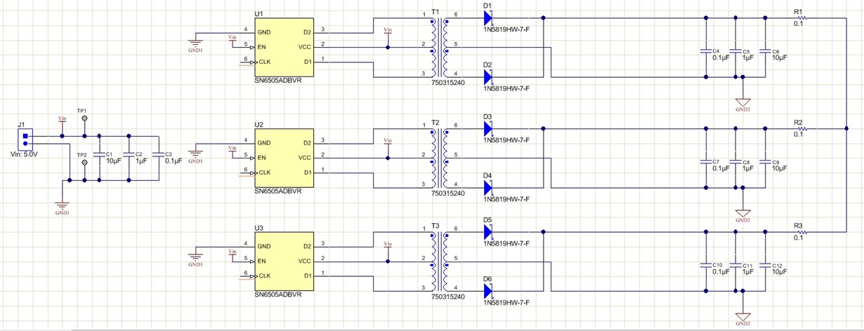
Can I take three identical SN6505B blocks (along with transformers, etc) and connect their outputs in parallel?

Do I need to make some magic with CLK input (provide external clock, etc), or SN6505 running on it's own internal clock (spread spectrum is still useful) is ok?

Maybe just add some bulk capacitance to the output (like 220-470uF) will smooth current spikes and reduce stess?

I've some concerns regarding diodes positive temp coefficiet that can lead to uneaven load distribution.

I can add three diodes to each block output to spread load more evenly.

Any suggestions?

Thanks,

Dmitry

  • Some update:

    I guess average current will be about 1.5A-2A (for three SN6505B connected in parallel).

    2.5-3A output may be needed only for short periods of time less than a second, during some transients in a system.

  • Hi Dmitry,

    This should be possible by tying the outputs of the modules together.
    Let me get back to you on this with a schematic and some calculations to back it.

    Regards,
    Anand Reghunathan
  • Hi Dmitry,

    For the SN6505 we have seen an output variation of <100mV across devices.
    Assuming typical value of diode and transformer series resistance, the resistance seen from one output to the next one is 0.7Ω when connected together.
    If we add a series resistance of 0.1Ω between the outputs the total becomes 0.7Ω + 0.1Ω = 0.8Ω.

    Current drawn between the outputs when the mismatch is 100mV (worst case scenario) = 100mV / 0.8Ω = 125mA. This current is well within the SN6505 limits.
    There would be a power loss across the resistances because of this current flow but it would amount to <50mW loss under worse case conditions.

    Please proceed with a schematic such as the one shown below to get the required current capability. The CLK input pin can be left floating and SN6505 can run using its internal clock.

    Let me know if you have any questions.

    Regards,
    Anand Reghunathan

  • Hi Anand,

    Thanks for so detail clarification.

    I'm checked again the SN6505's datasheet and according to Figure 11 graph, the output voltage swing for load going from 25mA to 1A is about 0.7V (like you said, 0.7 Ohm).

    So this voltage drop should work quite good in sense of load balancing between converters.

    Voltage drop is not a problem for me, I'm going to use TPS62030 buck-boost to stabilize the output voltage.

    Thanks,

    Dmitry