This thread has been locked.
If you have a related question, please click the "Ask a related question" button in the top right corner. The newly created question will be automatically linked to this question.
In looking at the F2803x datasheet, I'm trying to determine two things:
Let's assume that periodic self-recalibration occurs. It appears as though the INL and DNL are not additive. This would leave INL as the worst of the two at 4 counts. What I don't understand is whether what other errors are additive:
In summary, I'm trying to understand what all goes into determining the absolute worst case total unadjusted error, and what strategies can be deployed to minimize it?
Thanks,
Stuart
Hi Stuart,
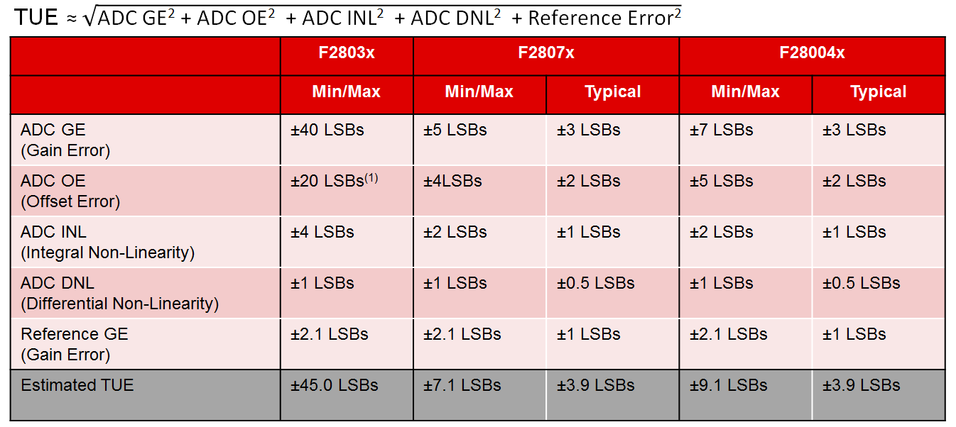
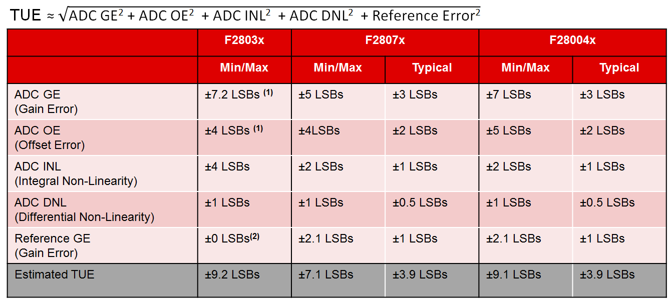
The first thing to look at is how we calculate total un-adjusted error (TUE). From the ADC we usually consider gain error, offset error, INL, and DNL. We also need to consider the error introduced by the ADC external reference. We don't need to consider ADC channel-to-channel offset or gain error, since this is just a measure of how much the channels can vary from each other (the worst case specifications hold for all channels).
The worst case ADC errors are usually independent (e.g. an ADC with worst case INL is unlikely to also have worst case gain error). Because of this we don't directly add the worst case errors, since this would result in an an overly pessimistic TUE. Instead, we add the errors using root-sum-squares.
Before we consider calibration, here is a comparison of the raw TUE of C28x Piccolo series ADCs. The specifications for F2803x, F2802x, F2806x, and F2805x are similar, so they don't all have their own table entry. Note that in all C28x datasheets, the Min/Max ADC errors are specified including drift for voltage, temperature, and manufacturing process variation. If a temperature coefficient is also provided, this isn't added on top of the worst case error (but instead gives some idea of how much of the error is due to temperature drift). Also note that the F2803x (and similar devices mentioned above) require at least one-time offset self-calibration (we don't support factory offset trim). All values in the table below are with external reference.
(1) Executing one-time self-calibration
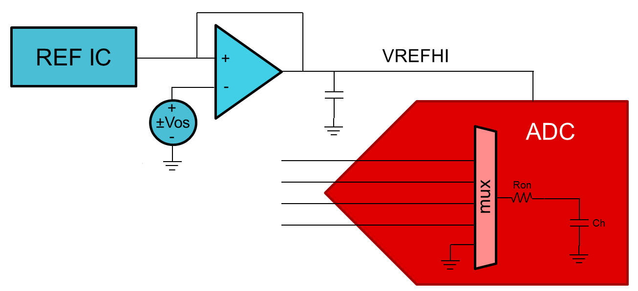
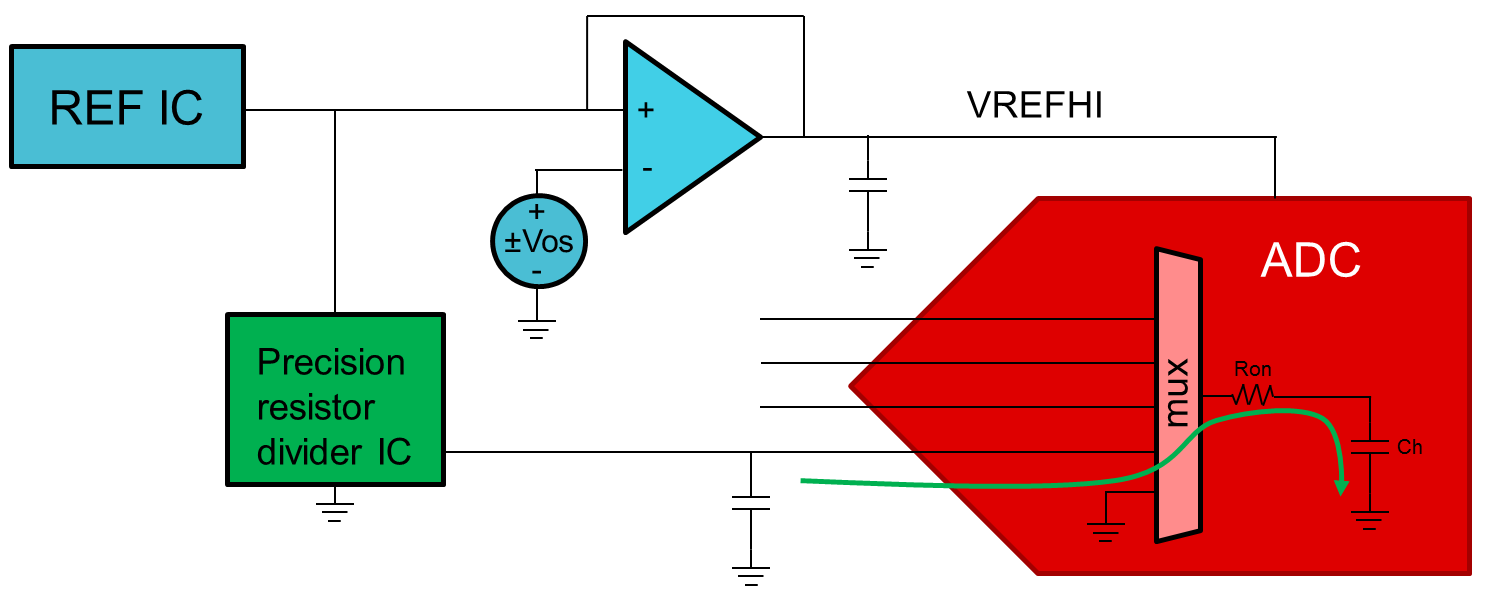
The external reference gain error has has some assumptions. This assumes a very good external reference solution.
For example, REF5030 has the following key specifications:
And then OPA320 (which we recommend to drive the 12-bit reference on F2807x and F28004x) has
So the total worst case reference error can be estimated as sqrt(2^2 + 0.7^2 + 0.2^2) = 2.1 LSBs (and 1.0 LSBs is just a guess for typical reference error).
Obviously if a different reference solution is used, the actual accuracy can also be calculated. Getting something more accurate than the above example is possible, but will get very expensive very fast.
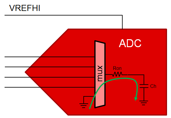
Now to calibrate offset error all of these devices have an internal connection to VREFLO (no external channel required). In the F2803x datasheet we specify +/-20LSBs with one-time offset calibration. To get better performance we can calibrate periodically:
Procedure: Sample the internal VREFLO connection periodically. Use these samples to adjust the ADC offset trim register accordingly. Adjusting the HW trim register will adjust the ADC samples directly, so no additional SW post-processing is necessary.
Limitations: Channel-to-channel offset variation will limit how close we can get to perfect offset trim. On F2803x, the channel-to-channel offset is specified as +/-4 LSBs.
Requirements:
Note: If the offset error is negative, the ADC conversion of VREFLO will read 0 and you won't know if the true offset error is -1 or something like -20. If you are periodically calibrating offset error on-line, the easiest way to handle this is to trim towards an offset error of +1 instead of 0. If the offset error is large and negative, successive rounds of calibration will eventually drive the offset error to +1. You can then either accept the extra 1 LSBs of error, or you can use the CPU to post-process the results. ADC range will be reduced by 1 LSB.
Calibrating gain error is a little more involved.
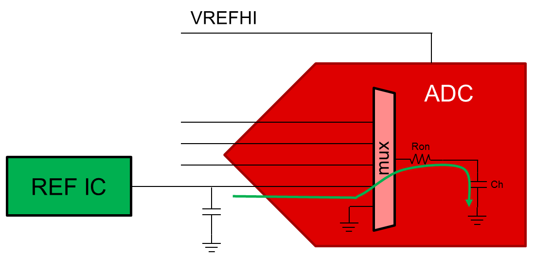
Procedure: Provide a single calibration voltage near the full-scale range. Since we already have an internal method to calibrate offset error, we don't need to do 2-point gain trim. Practically, using more calibration points will help average-out INL errors. This calibration voltage should be sampled periodically. The CPU can then post-process the ADC results to remove the gain error.
Limitations:
The error from sampling the calibration signal comes from a few sources:
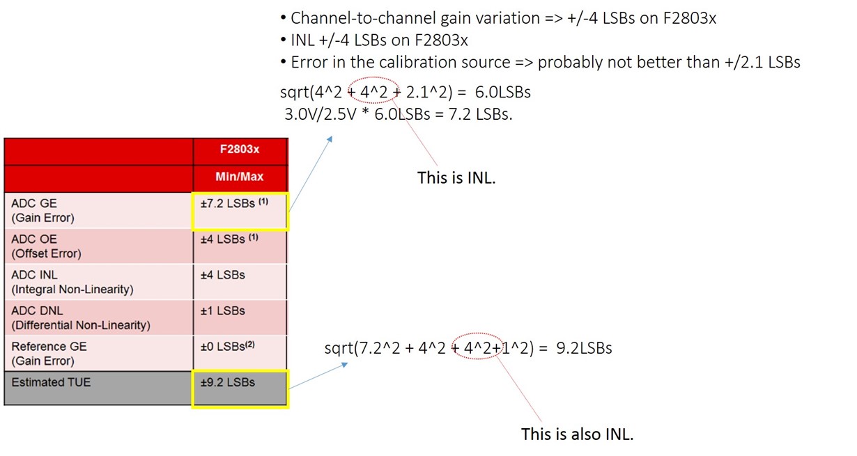
The best we can do for sampling error of the calibration voltage is therefore sqrt(4^2 + 4^2 + 2.1^2) = 6.0LSBs
The error at full scale range scales up based on where the calibration was done. So if the FSR is 3.0V and the calibration voltage is 2.5V, the total gain error would therefore be 3.0V/2.5V * 6.0LSBs = 7.2 LSBs.
Note: Because of the above, we want to do calibration as close to full-scale as possible. However, there needs to be enough space between full-scale and the calibration voltage to allow for any uncalibrated drift. For F2803x, the natural gain error is 40 LSBs = 30mV @ 3.0V VREFHI.
Requirements:
We can now fill back into the table the errors for F2803x with on-line calibration:
(1) Executing periodic re-calibration
(2) Error Included in ADC gain calibration
Some other notes:
Hi Devin-san,
I have 2 questions above.
Q1) Is not DNL unnecessary in the following formula? Because DNL is included in INL.
In the description of the link below, INL was not included
https://e2e.ti.com/blogs_/b/precisionhub/archive/2014/10/14/adc-accuracy-part-2-total-unadjusted-error-explained
Q2) TUE(F2803x ±9.2LSBs) calculates by the above method, but is it necessary to include INL in TUE calculation?
As ADC GE(F2803x ±7.2LSB) calculates including INL, I think that INL will overlap if INL is included in TUE calculation.
Best regards,
Sasaki
Hi Devin-san,
Thank you for your detailed answer !
I understood it thanks to your comment :)
Best regards,
Sasaki
Devin,
After implementing the code to check the trim register value and see that with temperature variation from 0 degree to 85C, the trim register value showed a 4LSB shift. I have some additional questions for you :
Thanks,
Stuart
Stuart,
Stuart Baker said:1. The datasheet specified a +/- 20 LSB offset error for the ADC . With the execution of the periodic calibration this error is supposed to be +/- 4 LSB. Please confirm.
correct
Stuart Baker said:2. How does the offset error exactly vary with temperature. Is it relatively flat in the temperature ranges of our interest (0-85C) and sharp increase/decrease at the allowable operating temperature extremities of the piccolo? The reason I am asking this is that we only see a 4 LSB shift and not the +/- 16LSB shift with temperature variation of 0-85C.
From the data I have reviewed, offset seems pretty linear across temperature, but the LSB/degC can vary fairly significantly device to device and can be positive or negative.
Stuart Baker said:3. All of our data was from a single piccolo. Does the +/- 20LSB factor account for part to part variation, ADC channel to channel variation ( or any other process factors) ? Can you elaborate the conditions from where the 20LSB number comes from. We suspect that the 20 LSB error accounts for the worst case conditions and since we are not operating in those conditions we don’t see the error.
The 20LSB represents the worst case drift seen across devices from multiple fablots, taken at different supply voltages and ADC conditions. It does not include ch2ch offset. It is certainly possible that some devices do not vary this much depending on the silicon and system conditions.
Regards,
Joe