This thread has been locked.

If you have a related question, please click the "Ask a related question" button in the top right corner. The newly created question will be automatically linked to this question.

LM5155: SEPIC topology, excessive MOSFET heating

Part Number: LM5155
Other Parts Discussed in Thread: LM3478,

Hello

I recently have been in contact with you regarding simulation problems when using LM3478 in SEPIC topology. However, I wanted to use the LM5155 for my design and you gave me the transient model for it to simulate the circuit.
https://e2e.ti.com/support/power-management/f/196/p/855129/3184699?tisearch=e2e-sitesearch&keymatch=lm3478%20simulation#3184699

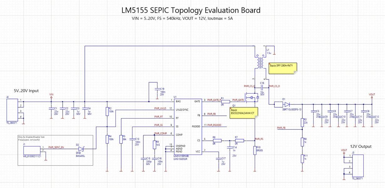
In the meantime I made an evaluation board to test the SEPIC circuitry with LM5155. I did the calculations/dimensioning according to AN-1484.

Requirements are:

Vin = 5..20V, Vout=12V, Ioutmax=5A

Calculations gave me:

L1=L2=700nH (coupled) (used SRF1280A-R47Y)

You can see the other components used in the schematics below. I encountered several problems which I’d like to share and also hope for some tips to improve the circuitry. Can you see any major dimensioning errors?

Problems:

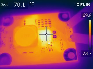
When drawing Iout=1A (far from the maximum), the Mosfet (type BSC022N04LSATMA1) already heats up to 85°C in appr. 2min. The power dissipation in the Mosfet is far too high. According to my calculations with Iout=1A, the Mosfet power dissipation should be 226mW. However, 226mW should not lead to such heating of the component, hence I assume the switching losses to be higher than expected. I’m aware, that the Mosfet on my board is not mounted on a 6cm^2 copper square as cooling area (as stated in the Mosfet datasheet to have RthJAmax=50K/W).

Of course lowering the switching frequency could be an option, however I’m interested in understanding the differences between the calculations vs. evaluation board.

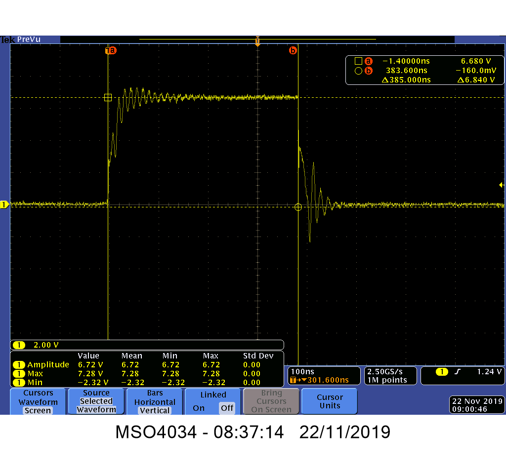
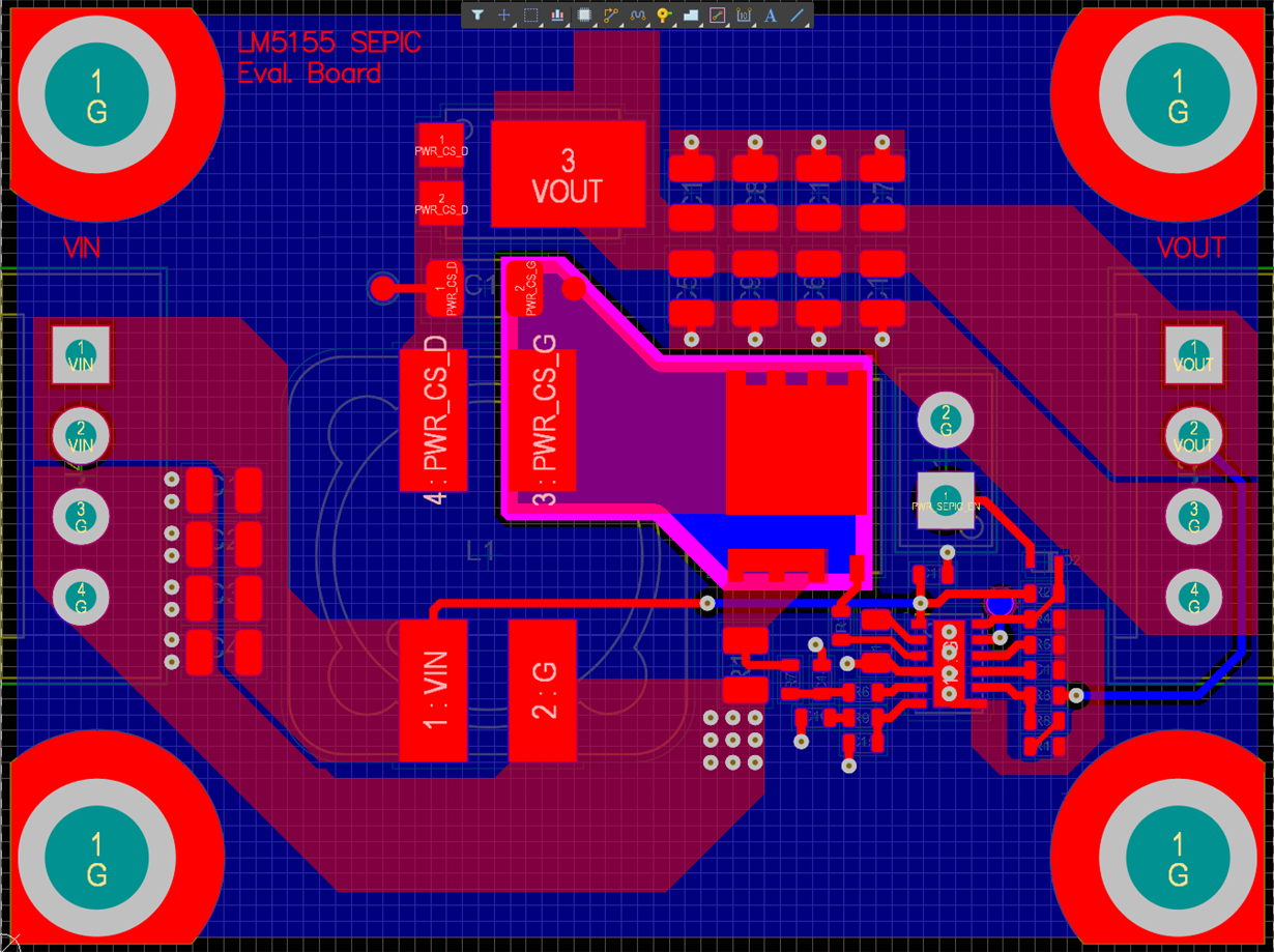
Measuring the gate voltage of the Mosfet, I observe more or less steep edges, but gate ringing exists. Gate ringing usually exists due to parasitics along the gate loop. However, the gate loop in my layout is quite small, the connection from the converter to the gate also. Do you have an idea where this gate ringing comes from? I also added my layout below.
Inserting a gate resistor to damp the ringing did not help, since it also slows down the rise of the gate voltage (and the longer switching time led to even more power dissipation in the Mosfet).
Do you have an idea where this gate ringing comes from and how to deal with it?

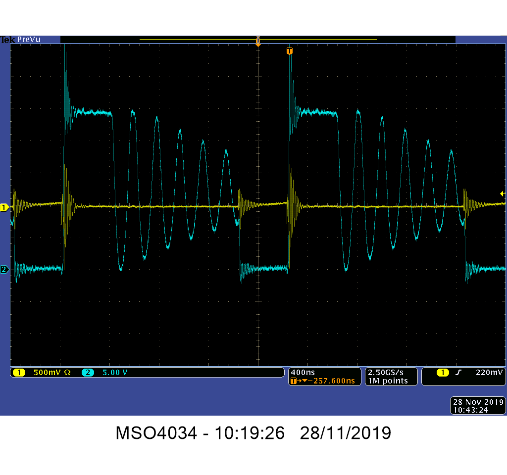
I also measured the drain voltage of the Mosfet (CH2) and the voltage across the sense resistor (R10). I assume the oscillations/noise to come from the grate ringing.

Simulation of the circuit did not show such behaviour and worked quite well. Please find the circuit also below.

Thanks in advance for any help!

Best regards,

Martin

LM5155-Q1_TRANS_SEPIC.TSC

  • Hi Marin,

    the experts supporting this device is out of office because of the thanksgiving holiday. the question would be answered when they are back to office next week.

  • Hi Martin,

    I just came back to office and I will take a look in the next two days, and reply to you.

    Thanks,

    Youhao

  • Hi Youhao

    Any news on this?

    Best regards, 

    Martin

  • Hi Martin,


    I might have confused myself with another task in my action items as this I marked "responded" last week. Sorry for the delay.

    The model that you simulated is 4.7uH.  You choose 0.77uH, which do not appear to be an appropriate selection.  You can see from the waveform that you circuit runs in deep DCM owing to the smaller inductor. The smaller inductor leads to higher ripple current, and hence higher RMS current and losses in the MOSFET and inductor.   Can you replace the coupled inductor with 4.7uH ones?

    Thanks,

    Youhao

  • Hi Youhao

    I'm a bit confused about some things you mentioned.

    >> The model that you simulated is 4.7uH.

    I actually have a 0.94uH coupled inductor in the simulation?

    >> You choose 0.77uH, which do not appear to be an appropriate selection.

    I calculated the size of the inductor following AN-1484. Calculations resulted in:

    L1=L2=0.7uH (coupled) 

    Using parameters: Vin=5..20V; Iomax=5A; fsw=540kHz; Vout=12V; Vd=0.3V

    Hence I've chosen SRF1280A-R47Y, where 0.47uH is the value of the parallel rating of the two inductors, hence one inductor is 0.94uH, which seems to be an appropriate selection when calculated 0.7uH.


    >> Can you replace the coupled inductor with 4.7uH ones?

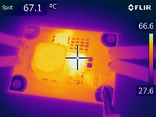
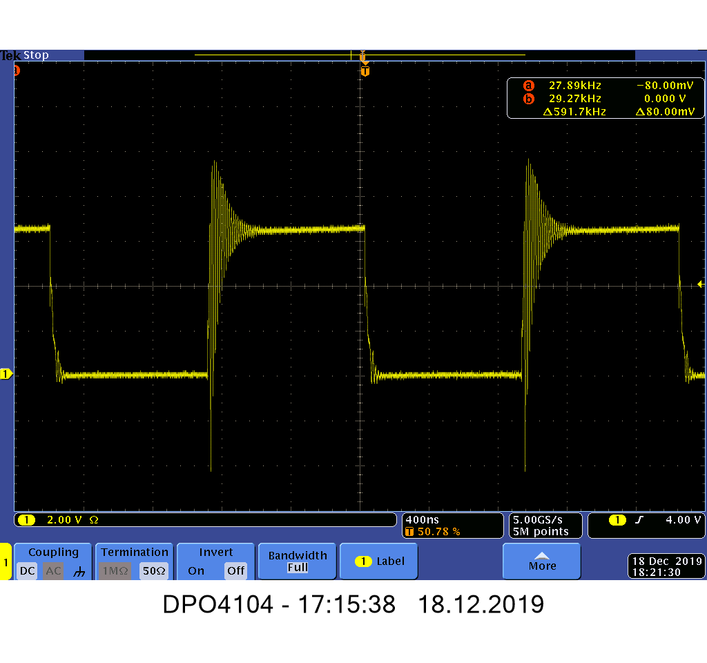
    Yes, I did. I now have an SRF1280A-4R7Y equipped, where one inductor is 9.4uH. This indeed led to less heating in the MOSFET. I still have around 67°C after 10 minutes, drawing Iout=1A (still far away from what is required). Also the gate ringing seems to be even bigger. Please see pictures below.

    Am I calculating or doing something wrong?

    Thanks in advance and regards

    Martin

  • The ringing is too much.  Can you increase the gate resistor from 0 Ohm to 2, and 5Ohm (please test both), and see any improvement?

    You also need to add heat sink to the MOSFET to help cool it down. There are  both conduction and switching losses in the MOSFETs.  

    Thanks,

    Youhao

  • Hi Youhao

    Just tested with different gate resistors:

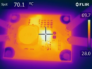
    Rg=2.2Ohm resulted in more excessive heating than with 0R (70°C after 5min). Also the gate resistor gets almost as hot as the MOSFET. See measurements below:

    The gate ringing was not damped drastically.

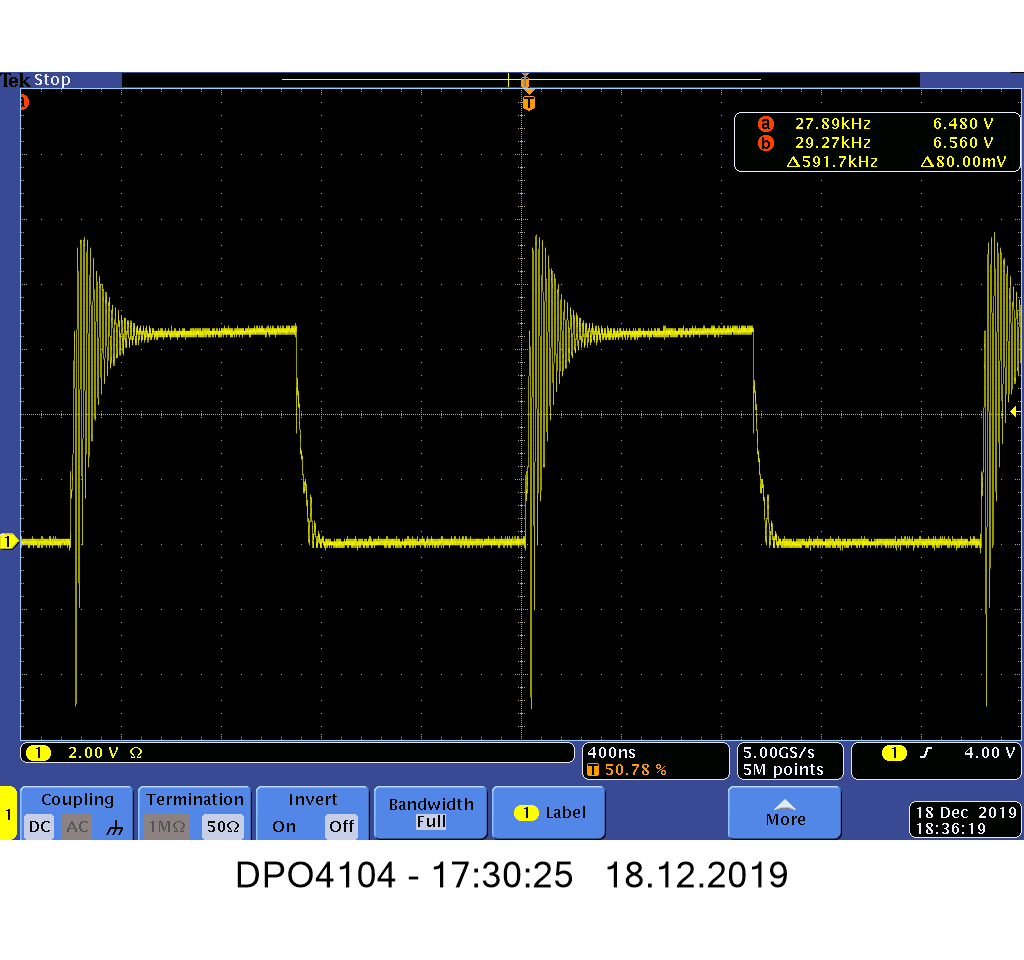
    Rg=4.7Ohm resulted in even more excessive heating than with 2.2Ohm (70°C after 3min). Also the gate resistor gets almost as hot as the MOSFET. See measurements below:

    The gate ringing was also not damped drastically.

    I know I didn't have a heat sink on the MOSFET on this test. I was assuming to be able to generate more output power without such excessive heating of the MOSFET even without heat sink.

    Best regards, 
    Martin

  • Hi Martin,

    You should consider to change your layout to make the ac current loop compact and small. You existing PCB has large ac current loop:  Cout --> Rsense --> MOSFET--> Switch node --> Cout.  This loop should be direct and short distanced.  I would rotate the MOSFET by 180 degree, and place the Rsense close to the Cout ground pad.  Therefore, the parasitic inductance can be greatly reduced to avoid severe ringing at switching edges.

    For the time being, you can try to add an RC snubber across the MOSFET drain and ground at the Rsense and see if the ringing can be suppressed. 

    Also, please use the design calculator to help calculate the MOSFET losses, then do a thermal assessment.  

    https://www.ti.com/lit/zip/snvc224

    Thanks,

    Martin

  • Hi Youhao

    I agree, the as current loop should be smaller. However, rotating the MOSFET by 180 will on one hand improve the ac current loop, but worsen the switching signal loop (GATE -> MOSFET -> RS -> GND -> GATE). I think I have to consider new an better placement for the next test board.

    I will try the RC snubber suggested in January and then let you know about the results.

    I tried calculating the MOSFET losses with your quickstart calculator and ended up at approx. 200mW at Iout=1A, which is more or less the same as with the calculations according to AN-1484. This doesn't match with the measurements done unfortunately.

    Thank you for the help provided in this case and wish you merry christmas!


    Best regards, 

    Martin

  • Hi Martin,

    If you rotate the MOSFET, you can re-route the gate trace.  The traces to the Gate and the return trace from the ground pad of the current sense  back to IC PGND pin, can be tailored such that the gate drive current loop does not enclose much spatial area.  The gate and return traces can be routed closely side by side to minimize the spatial area, then the drive signal should be okay. 

    Thank you for your kind words, and wish you, too, a Merry Christmas and a Happy New Year!   

    Best Regards,

    Youhao