This thread has been locked.

If you have a related question, please click the "Ask a related question" button in the top right corner. The newly created question will be automatically linked to this question.

Supplying TPS61200 with a single solar cell

Other Parts Discussed in Thread: OPA379, TLV431, TPS61200, BQ24071, TPS63000, TPS63010

Dear all,


Thanks you for taking the time to read my post.


I am interested in building the circuit described in “Supplying TPS61200 with Solar Cells”, for a solar battery charging application.


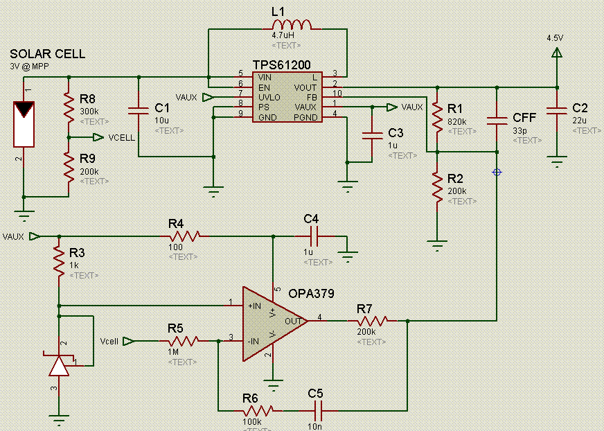
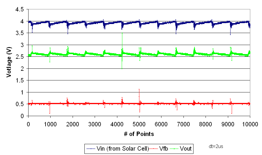
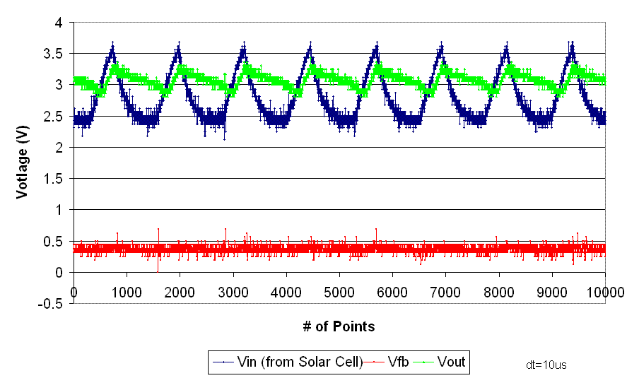
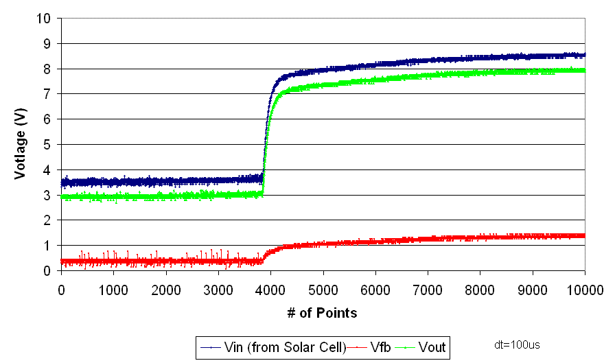
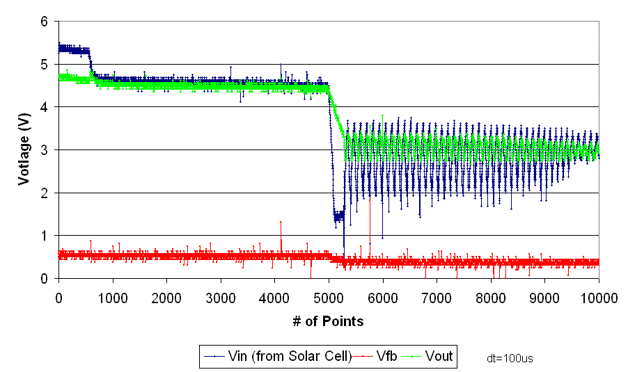
However, the document does not give an indication as to how it calculates the values of some of the components, in the figure below.


I am interested in building the circuit, that will provide a Vout of around 4.5V, from a solar panel voltage (@MPP) of around 3V.


Any help would be much appreciated.


Thanks and regards

Alex

  • Hello Alex,

    mainly this circuit is designed to be driven by a single solar cell (0.4 to 0.6V). The reference TLV431 provides a voltage of 1.24V therefore you need to divide the solar generated voltage with a divider to a voltage below 1.24V. Otherwise the MPP circuit will not work. If you connect the positive input of the OPA379 directly to VREF R4 is not needed anymore.

    To get an output voltage of about 4.5V you will need 820k for R1. The output voltage can be calculated as described in the datasheet with just a slight change.

    R1 = (R2||R8)x(VOUT/VFB - 1)  with R2||R8 = 100k  

    Best Regards

    Andreas

  • Thanks for your reply Andreas.

    I am not very familiar with shunt regulators, or the exact workings of the TPS61200 IC feeedback loop.

    I have thus attached a schematic of what I think you meant by your post.


    I would be grateful if you could give me some feedback.

    Thanks and regards

    Alex

  • Hello Alex,

    your schematic looks good and should work fine. I would prefer to use 680k for R8 and 470k for R9. This is closer to 3V and gives you better efficiency.


    Regards Andreas

  • Thanks for your reply Andreas.

    I now have a question regarding the schematic below. As I said in my original post I am interested in a solar battery charging application. I have been thinking of using the TI’s BQ24071 in this application, which provides DPPM (Dynamic Power Path Management) on the output pin.

    I am not sure if you are familiar with the chip, so I will try and ask the question as simple as possible.

    When the solar panel is not producing enough current to satisfy the system load, the BQ24071 will try and pull its Vout pin to the battery voltage (It will try and supply the load from the battery). By consequence the input pin of the BQ24071 will be pulled to battery voltage and so will the output pin of the TSP61200 converter. What would happen in this scenario?

    It seems to me that there might be a conflict between the TPS61200 trying to maintain its output voltage (to say 4.5V in my case) and the BQ24071 trying to pull down its input and output voltage to anywhere between 2.8-4.2V.

    Ideally I would still want to supply current to the load, even if it’s not enough to cover the whole demand. Any on what would happen and how I could mitigate such a problem?


    Thanks and regards

    Alex


  • The TPS61200 would try to draw more current from the solar cell, thus decreasing the cell's voltage.  At some point, your MPPT circuit will kick in and reduce the TPS61200's target (regulation) voltage, thus allowing an equilibrium to exist between the solar cell's voltage and the TPS61200's voltage.  The additional current needed to power the system would come from the battery.

  • Thanks for your reply Chris

    I was under the impression the golden rule of control theory was never to have two separate control loops.

    Ideally I would like to completely isolate the TPS61200 circuit from the 'Power path management and battery charging' IC. Having the BQ24071 pulling down the solar panel voltage will considerably reduce the efficiency of such a solar powered battery charger.

    Does TI offer a 'Power Path Management and Battery Charging' IC that will not drag its input voltage to battery voltage when the load current exceeds the power source current?

    Thanks and regards

    Alex

  • "Does TI offer a 'Power Path Management and Battery Charging' IC that will not drag its input voltage to battery voltage when the load current exceeds the power source current?"  Pulling down the input bus actually makes things more efficient.  In a linear charger, only the amount of current pulled from the input matters.  The voltage of the input simply results in excess power being lost in the pass element in the charger IC.  So, if the input is current limited, the IC will pull down the voltage in order to get the most current from the input--typically, as the input voltage droops, the current that it can deliver increases--just like a solar panel.  So, running the output (and input) at the battery voltage gets the most current out of the input source and wastes the least power in the pass FETs in the IC, as all of them are fully on.

    Pulling down the output of the TPS61200 is the same thing as described above.  The MPPT circuit will operate the panel at its maximum power point by reducing the output voltage as needed.  This input power from the panel will give an output power of some amount based on how much current the charger/system takes.  Most likely, this output current will be less than needed to fully fast charge the battery, so the charger IC will pull down the output voltage to get the most current from the TPS61200.  This constant output power (lower output voltage and more output current), still comes from a constant (maximum) input power from the solar cell.

    I encourage you to build up the various pieces of this circuit and see how it behaves for your application.

  • Thanks for putting the effort in replying to my questions Chris.

    I am interested in understanding the comparator circuit (and the feedback operation it provides), with the intent on adding a potentiometer as part of the resistance of input voltage divider (either top or bottom or both).

    My intent is to evaluate how 'sensitive' the feedback circuit is, thus having a future possibility of adding a SPI controlled resistor in the future for a complete MPPT system.

    However, I lack the knowledge to arrive to the fundamental equations that describe the comparator feedback system.

    I would be grateful if you could point me in the right direction.

    I am specifically trying to understand how a change of the input voltage divider output, affects how much current is drawn from the solar panel. I have gone to some length to try and understand boost converters and average current mode control (which is what the TPS61200 is using).

    I have found TI documents Control Loop Cookbook, Average Current Mode Control of Switching Power Supplies by Lloyd Dixon an excellent start. However, I am not at point where I can derive what I need myself.

    I have trouble finding all of Lloyd Dixon’s documents on switching power supplies under the ‘Search Technical Documents’ umbrella. I can find them through Google (on not TI websites), but not through TI technical search engine. Is there somewhere else on the TI website Is should be looking? I am just asking, so that I do not miss something important.

    Any help would be much appreciated. If you could point me to other excellent documents like those listed above that might help me, I would be eternally grateful.

    Regards

    Alex

  • So, the MPP circuit works by looking at the divided down cell voltage, comparing this to a reference (TLV431), and then adding or subtracting current to the FB pin of the TPS61200.  The OPA379's current sourced or sinked through R7 has the result of tricking the TPS61200 into thinking the output voltage is higher or lower than it should be.  The TPS61200 adjusts its duty cycle and thus the real output voltage (on Vout) accordingly.  So, if the cell voltage is too low, the OPA379 output will go higher and source more current into the FB pin.  Thus, the voltage at FB will rise and the TPS61200 will reduce the duty cycle, lowering the output voltage.  This lowers the output power and thus the input current.  Thus, the cell voltage rises back up.

  • Thanks for your reply Chris.


    You reply provided me with a better understanding of how the circuit works.


    However, what I had in mind was a more detailed explanation.


     I am trying to understand the relationship that exists between the voltage divider output and the current being drawn from the solar cell.


    The figure below shows how the output from voltage divider reduces, as resistance R1 is increased in 780Ohm steps. I am assuming a R1/R2 of 680k/470k voltage divider, with an additional pot in series with R1. The figure assumes a pot of 200k in series with R1 (this value also corresponds to a SPI controlled digital resistor).


    I am asking this question, as I am in the process of designing the PCB with the TPS61200, OP379, BQ24071 + buck-boost converter + load. It would be helpful to me if I knew whether I need 'large' changes in the voltage divider output, to affect the current drawn from the solar cell, or 'smaller' ones (i.e. do i use a 50k, 200k or 1M potentiometer ?).


    Regards

    Alex

  • I assume R1/R2 is really R8/R9 in the third post.  Per the app note, the purpose of that divider is to generate a voltage equal to the reference voltage (TLV431 voltage) at the MPP of the panel.  Thus, you pick 2 resistors that divide down the MPP voltage to the reference voltage.  The POT is only needed to tweak the circuit and to provide an easy way to change the MPP and see the resulting operation.  What value POT to use is up to you.  One way to look at it is to take the maximum and minimum resistance values of the POT and see what cell voltage the resulting divider will give you.  With a 680k upper resistor, I would think a 50k POT would do well.  If you really want to zero in on the MPP, then a smaller value POT with more turns would be better.

    If you haven't already, take a look at the TPS63000 family for your buck/boost converter.

  • almost_linear said:
     I am trying to understand the relationship that exists between the voltage divider output and the current being drawn from the solar cell.

    The MPPT circuit will ensure your solar panel is close to its maximum theoretical efficiency given the light and temperature condition at which it is operated by adjusting its output voltage.

    To know the current being drawn from the panel you'd need to look at the voltage/current characteristics of the panel identify the voltage at which it offers maximum efficiency (the one you will be tuning the circuit for) then look on the graph for associated current.

    You may want to look at (SLUA394) for more details on those aspects.

    Hope this helps,

    BR,

    MCV

  • Hi,


    I have just built the block diagram as shown in the figure in post 5. This consists of the TPS61200 with a MPP circuit (soft start), followed by the BQ24071 battery charger and power path manager and finally the LT3440 buck boost converter.


    Since I have been getting problems only with the TPS61200 circuit I have decided to isolate it from the rest and test it on its own.


    I have connected a 100 Ohm resistor as a load and a 10 Ohm resistor in series with a power supply, to simulate the solar cell. Load resistor was choosen slgihtly arbitrarily by me. The application report SLVA345A does not really mention what load they tested there circuit with. On page 5, last paragraph it is mentioned: "...the load current at the output of the converter is set to 1mA." Does this mean the load used was a 3.8 kOhm resitior (3.8V/1mA)?


    I have set the input voltage to 4V and output is meant to be boosted to 4.5V.


    From the figures below one can see that the TPS61200 is not boosting the input voltage. If I increase the input voltage, the TPS61200 will track quite well, but it will not boost the voltage.


    The pot has been set to 0 Ohms.


    The TPS61200 schematic along with some measurements I took, can be seen in the figures below.


    Any advice would be more than welcome.


    Regards

    Alex


  • The TPS61200 is properly regulating to its setpoint--2.5V.  R1 and R2 set this voltage.  Most likely, the MPPT circuit is always feeding some current into the FB node which would alter the voltage on the pin and cause the TPS61200 to regulate to a different level.  I also noticed that C_GND and P_GND are not shorted anywhere on the schematic.  This is required.

    Is there any particular reason why you are using the LT3440 over the TPS630xx series?  Our parts have the compensation network built in, which makes it a lot easier to design with.

  • Hi Chris and thanks for your swift reply.


    Control ground and power ground are connected at pin 4 (PGND) and only there.


    The tps63010 looks interesting, but I have used the LT3440 before and it meets my requirements for now. If I were to re-design the PCB I might think of changing to some other buck-boost converter.


    Not quite sure what you mean by “The TPS61200 is properly regulating to its set point--2.5V.  R1 and R2 set this voltage”.


    As far as I understand R1 and R2 set the output voltage which should be at 4.5V. Also the feedback pin ‘fb’ is around 500mV (see figure 3, 4), which according to the manual is its nominal value for regulating.


    Do you have any idea at what load this circuit was tested at according to the application report SLVA345A.


    Regards

    Alex

  • Correct, R1 and R2 set the output voltage.  In your schematic, R1 = 820k and R2 = 200k.  This voltage divider takes the output voltage and compares it to the 500 mV reference.  Thus, your output voltage is set to 2.55V.

    Page 5 of that app note says: "The following illustrations show the TPS61200 start-up behavior with and without the MPP circuit. For both illustrations, the load current at the output of the converter is set to 1mA"

  • Am I being thick? In my circuit schematic R2 and R7 (both 200kOhm) are in parallel (according to Andreas post). Thus R2||R7=100kOhm.

    If I am wrong, what values should R1, R2 and R7 (in my schematic) take, to get an output voltage of 4.5V?

    The app note (both the August and October version) say 1mA. Thus, the authors must have used a 3.8kOhm resistor if they were boosting to 3.8V. If this was a typo and they meant 1A, then they used a 3.8 Ohm resistor (???).

    Regards

    Alex

  • If you removed the TPS61200 from the rest of the circuit, R7 is floating and not connected to ground on one end.  Thus, it is not in parallel with R2.  Your FB voltage on your plots is at 500 mV.  Thus, the IC is regulating properly.

    There were some format issues in my last post.  Yes, 1 mA is what the app note says they used for a load.

  • What values then, should R1, R2 and R7 (in my schematic) take, to get an output voltage of 4.5V?

    It seems a bit odd to me to draw 1mA from a converter, that can supply at least 300 times that. Could you maybe provide some light as to the motives fo the authors on this?

    Thanks and regards

    Alex

  • For a standalone TPS61200, the output voltage is programmed as described in the datasheet or previously in this post.  Just change the 200k resistor to 100k.  Or just ground R7.

    As described in the app note, 1 mA is a typical operating current for the electronics/sensors used in a solar powered system.  Note that 1mA is just the load used at start-up.  The TPS61200 can support higher loads, but small solar panels may not be able to support these higher loads at all.

  • Hi Chris and thanks for your reply.


    I have replaced R2 to 100k and left R7 at 200k and I still get no boosting of the voltage. I have tried different loads of 3-70 Ohm, 100Ohm, 3.9k, 4.7k, but I still get no boosting.


    Will the TPS61200 with MPP circuit work for higher loads? If yes up to what currents can it go up to? I was under the impression the circuit I have shown would go up to at least 500mA. I made this assumption by looking at Figure 1 (p.6) of the TPS61200 datasheet.


    Regards

    Alex

  • Yes, the MPPT and TPS61200 circuit works to higher loads.  The main constraint is the size of your solar panel and how much power it can support.  Assuming it can support a fixed voltage at infinite current, then the TPS61200 can output a maximum current as shown in figure 1.  This case is limited by the TPS61200.  The real case is the solar cell supporting a fixed voltage up to some current.  If this current is above what the TPS61200 requires at its maximum output current, then again, the TPS61200 is the limiting component.  If the current capability of the solar cell is less than what the TPS61200 requires, then the MPPT circuit will kick in and reduce the output voltage of the TPS61200.  In this case, the limiting component is your solar panel.

    Try taking the same plots you did earlier, showing the FB voltage and output voltage and input voltage.  If the FB voltage is at 0.5V, then the IC is regulating properly to whatever you set its output voltage to.

  • Hi Chris,

    The figures below were taken with R2=100k, R7=200k and a load of 4.9k.

    It seems that with R2=100k, the Vfb has trouble reaching 500mV. As you slowly increase the voltage of the power supply (from 0V), you begin to get an oscillatory behavior (whose pk-pk voltage increases) . This oscillation then suddenly dies down after a point, and  soon after (after you continue to increase the voltage slowly) you get a big jump on VIn, Vout and Vfb.

    After this 'jump', if you begin to decrease the voltage you get a steep fall in all three voltages, followed by the same oscillatory behavior you saw in the beginning.

    Below are the waveforms.

    Hope you can provide some answers.

    Thanks and regards

    Alex


  • If you have truly disconnected the TPS61200 circuit from everything else, then R7 is not connected on one end and does not effect the circuit's operation.  Confirm that R7 and R6/C7 are not connected to the circuit you are testing.

    In the first picture, your input supply is oscillating.  Try testing without the 10 Ohm resistor in there and see if your input supply becomes stable.  It needs to be stable.

    In the second picture, you have violated the absolute maximum rating on Vin.  You probably destroyed the IC.

    Try replacing the IC, removing any impedance from your input supply and retest.  Or order the TPS61200 EVM. http://focus.ti.com/docs/toolsw/folders/print/tps61200evm-179.html 

  • Hi,

    Could you send me this schemtic file in order to simulate the circuit please ? it's urgent.

    Thank you in advance