This thread has been locked.

If you have a related question, please click the "Ask a related question" button in the top right corner. The newly created question will be automatically linked to this question.

BQ24103: IC potentially overheated

Part Number: BQ24103
Other Parts Discussed in Thread: BQ25601, BQ25600D, BQ25600

We have manufactured more than 30k units of our product using BQ24103.

There has been detected a charge error on some units and by investigating these units it is shown that the charging circuit BQ24103RHLR is broken. It looks like the IC is overheated and that a compound has leaked from the IC and formed a bubble, as can be seen on the attached picture. Schematics is also attached.
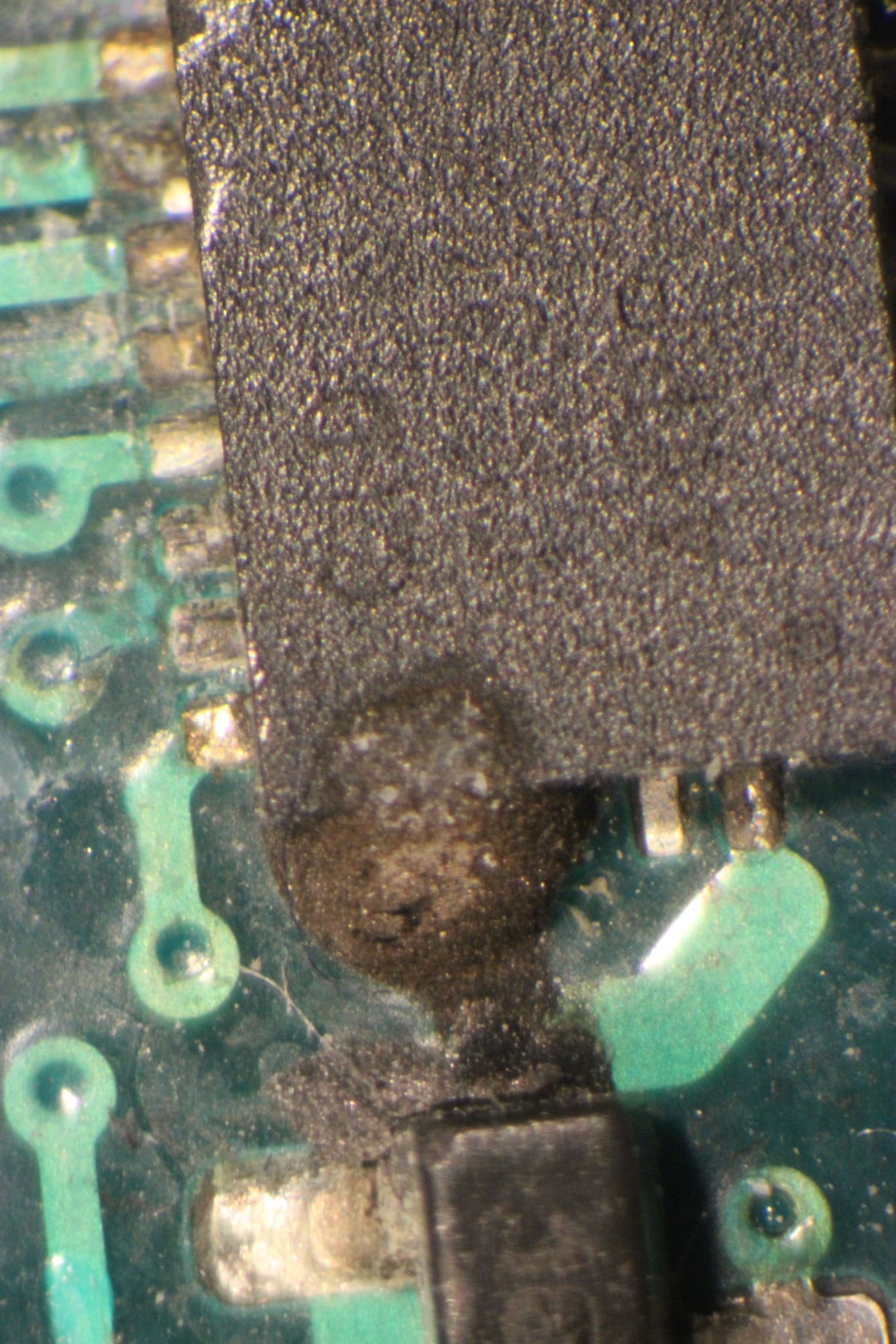
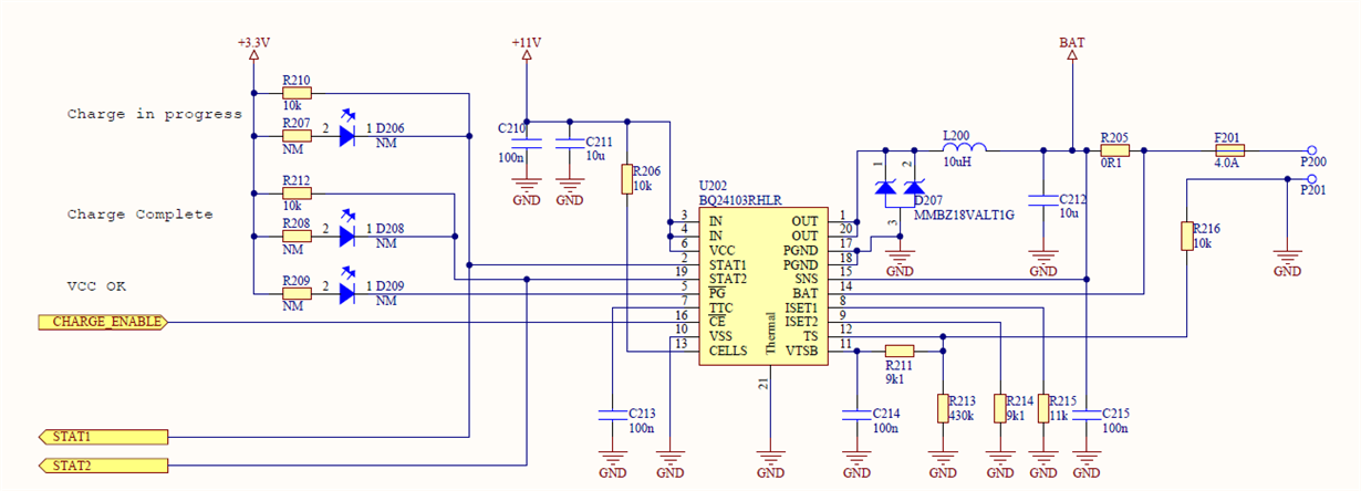
  Initially we do not expect that there is an issue with the IC, but we are very interested in finding the reason that this can happened. Especially since the circuit has over temperature protection.

 The product is molded and thus there is hard to search for the root cause. The molding must carefully be removed and this is a time consuming and difficult process that might inflect new errors on the board.

 Q1. Have you seen this symptoms before?

Q2. Do you have any suggestion on what might cause this error?

  • Hi,

    Apologies for the delay.

    On the units that have had this error, does the bubble occurr in the same location on the IC?

    What IC pins are located near the bubble?

    -Joe
  • Hi Joe

    Thank you very much for the reply. From the boards that I have inspected it looks like the bulb is always close to either pin 1 or pin 20.

    Looking forward to your response.

    Regards Audun

  • Audun,

    Okay so the bubble repeatedly occurs at the output. What is your maximum output current?

    You have CELLS tied HIGH so you have output set to 8.4V charge, correct? I want an idea of the amount of power your design is expecting.

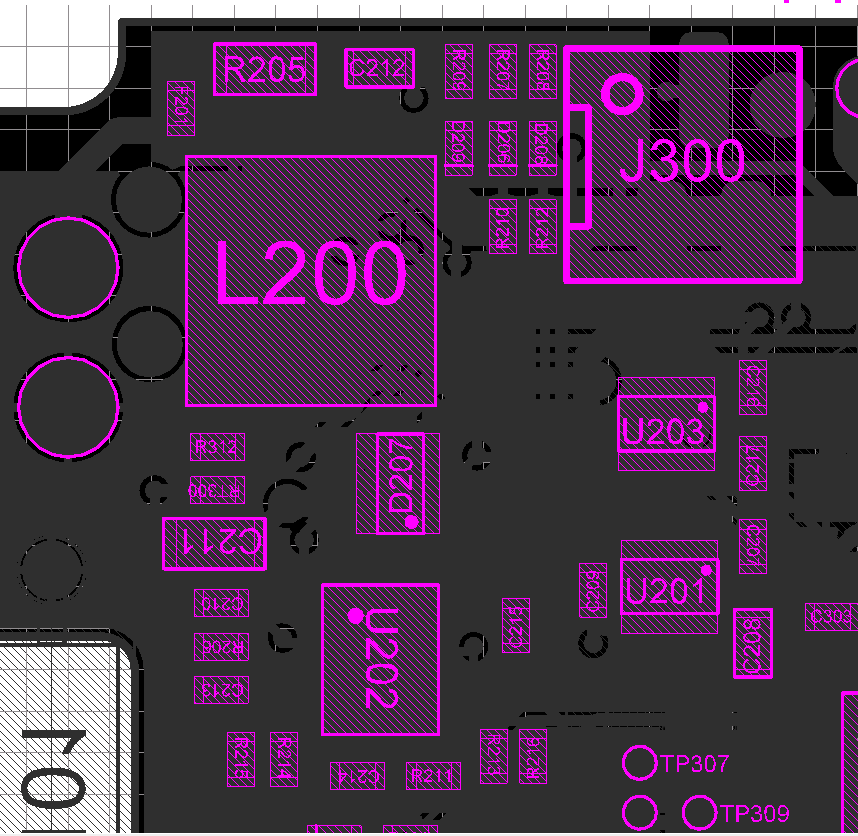
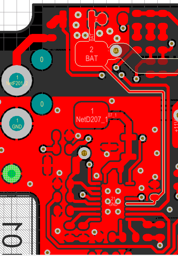
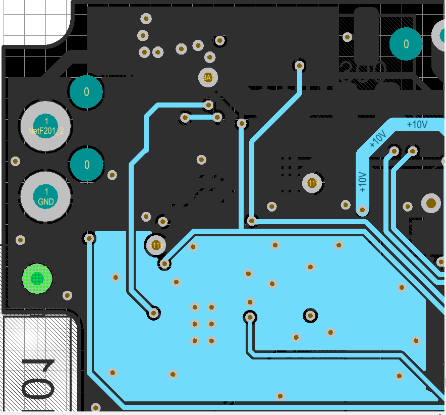
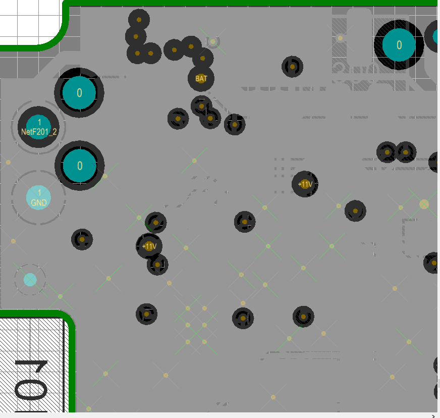
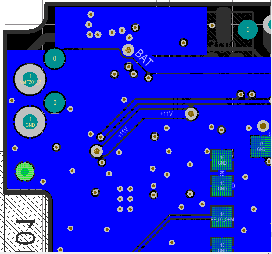
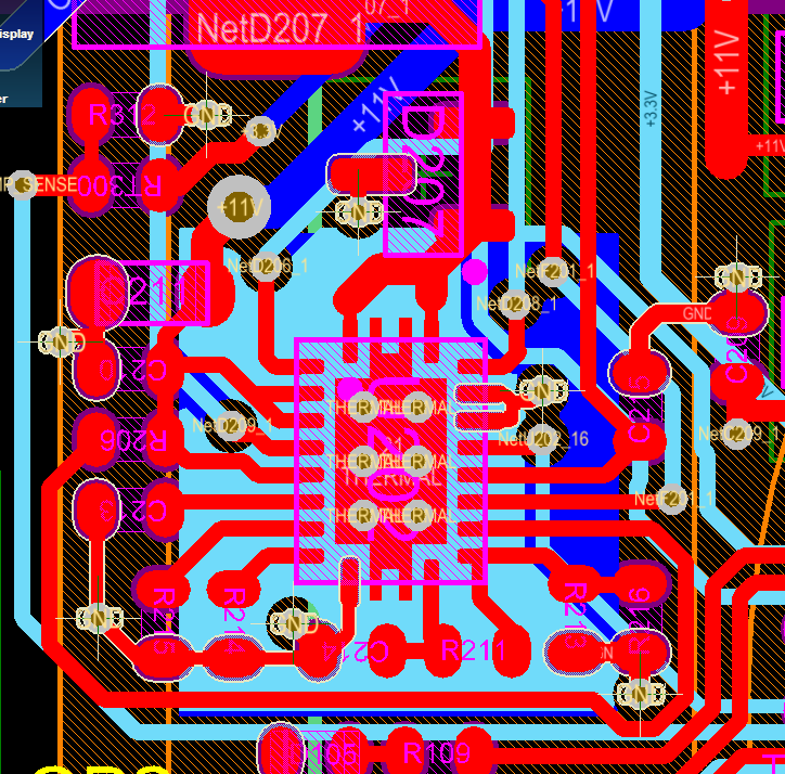
    Would you be able to share an image showing how you have this section of your board routed? Layout for these designs is very important for electrical and thermal performance.

    -Joe
  • Hi Joe

    Charge current is configured to 0.91A

    Yes we are charging a 2S1P battery with 8.4V.

    I have uploaded layout pictures, please let me know if you need more pictures.

    Since we have manufactured a lots of these boards there seam to be something that is marginal. Could a short under the IC due to bad soldering cause such an issue?

    We do really appreciate your support.

    Regards Audun

  • Audun,

    Thank you for the images. Allow me some time to take a look.

    Novice said:

    Since we have manufactured a lots of these boards there seam to be something that is marginal. Could a short under the IC due to bad soldering cause such an issue?

    This could be the case. While I take a look at the layout I suggest using a multi meter to try and detect a short from the output to another trace of the board. Also, a quick test that will help determine if this is an issue with the board is to take a bq24103 from a board that is working properly and put it on one of the boards that has the issue. When you do this, also observe how quickly the bubble event occurs.

    Regards,

    Joe

  • Thanks for the suggestions Joe.

    I will go ahead and check this.

    Regards Audun

  • Hi Joe

    I measured between OUT (pin 1 & 20) and GND on to failing units and both had a short.

    When I removed the IC the short was gone and I was not able to measure a short on the IC either. Could indicated soldering issues, but if that is the case it should had failed right away during production test.

    Should it be possible to measure connection between pin 17/18, 10 and 21 on the IC or are they all isolated?

    I have investigated some more and notice that the failure only occurs on an old batch were the layout did not have a connection between the thermal pad and GND, see attached picture. What would be the consequence of not having pin 21 connected to GND in the layout?

  • Hi Joe

    Can you provide more information for this case?

    I received an e-mail that Wang5577 had provided the following answer, but it does not appear in this tread:


    "Wang5577 replied to BQ24103: IC potentially overheated.

    I don't see any snubber or clamp circuit on "+11V" input. The damage pin seems the "IN" pin. What is the maximum input voltage spike during the input source hot plug-in?

    Please contact the quality team and send some failure samples back for failure analysis to confirm which pin got damage."

    I have a TVS Diode SM&T18A as an over voltage protection for the input. Pin 1 and Pin 20 are the damaged pins.

    Can you please send me contact information to the quality team such that I can send in samples for failure analysis?

    Regards Audun

  • Hi Audun,

    I apologize for the late response, I have been out of office for the recent holiday. Please ignore the post from Wang at this time. I don't beleive we have reached a conclusion that should involve the quality team at this time.

    Audun said:

    Should it be possible to measure connection between pin 17/18, 10 and 21 on the IC or are they all isolated?

    These pins are not internally connected.

    Audun said:

    I have investigated some more and notice that the failure only occurs on an old batch were the layout did not have a connection between the thermal pad and GND, see attached picture. What would be the consequence of not having pin 21 connected to GND in the layout?

    The Thermal Pad and VSS must be connected. VSS, PGND, and Thermal Pad sharing the same ground rids the IC of having ground bounce issues. Also, the high-current IN and OUT charge paths utilize the thermal pad for the return current. If this pad is not connected to GND, then it can't be used and all the return current is going through the VSS and PGND pins. It is very important to have the return paths go through the thermal pad in order to properly spread the heat accross the GND plane. If it is not connected, then you most likely have nodes of extreme heat on the VSS, PGND, IN and OUT junctions of the IC. This is what I believe is happening that causes the failure near the OUT pins.

    Please see page 32 in the bq24103 for more information on layout guidelines for the thermal pad.

    Regards,

    Joe

  • Hi Joe

    Thanks for the feedback.

    There are a couple of things that I feel don't match with this explanation. It is the OUT pins that are damaged and the current through these pins should be equal regardless of the Thermal pad being connected to the GND plane. If connection of the Thermal pad to GND is the cause I would expect the heat issue to be on VSS and PGND pins, but I do not see any issue on these pins.

    Another thing is the measured connection between OUT pins (pin 1 and 20) and GND on the failing units. Using a multimeter I could measure a short between GND and OUT. After removing the IC the short is no longer measured either on the IC or the PCB.

    Another thing is that I would have expected more units to fail if connection of Thermal to GND is the cause since this is implementation is similar on a large number of units.

    Do you agree that these findings do not match with the explanation?

    Regards Audun

  • Hi Audun,

    When you measured the short between OUT and GND, was the device powered? If so, measure without it powered. Could be that there is a short due to the failure when the device is powered only.

    I made a slight error in my earlier post. VSS and the thermal pad are internally connected. PGND is not. By not having vias to GND on the thermal pad, the current won't pass through the pad so the heat cannot be properly managed. This is most likey causing extreme thermal junctions within the IC. There is more resistance at the output pins, so this may be why the failure occurs there.

    Do you know how many units failed out of the total old units without the thermal to GND connection?

    This failure isn't happening on all of the boards without the connection, but there is no gurantee they won't fail the same over time. The datasheet mentions a couple times that the thermal pad must be connected to GND. Since this failure is only occuring on boards without the connection, the problem seems clear.

    -Joe
  • Hi Joe 

    I have been on vacation so sorry for the late reply.

    Yes the short was measured without power.

    The current going through the OUT pins should be equal regardless of the Thermal connection to GND so I still find it hard that this should be the effect of not connecting Thermal to GND. Instead I would expect the failure to occur at the VSS pad.

    I believe that there is approximately around 5% of the old version that have failed. It seams also like the failure is consecrated around a specific year and not evenly distributed above the years that this design was used.

    This is also an indication that there might be something else that is causing the error. Could a short under the circiut be the reason. E.G if the paste mask is worn out and to much paste is being applied to before soldering?

    Audun

  • Hi Audun,

    Its clear that the problem is related to thermal issues. The thermal pad needs to have good copper pour placement so that the IC can perform at the specifications on the datasheet. This will allow good thermal conduction between the IC junction and the GND planes in the PCB.

    The difference between the old boards and new boards suggests that the thermal pad layout connection is the main source of the problem.

    Regards,
    Steven

  • Hi Steven

    Thanks for your additional comment. I agree that the difference between new and old design indicates GND connection of thermal pad as the cause of the failure. The only thing that doesn't completely add up with this is that the failures are not evenly distributed among the production batches of the old boards. It is mainly boards produced in 2014 that are failing. This is one of the reasons that we suspect that it might be associated with the soldering process of the board or maybe worn out paste stencil.

    Parallel with this investigation we are looking for parts for the next generation. Next generation will use battery pack of 3.6V and we are considering BQ25601 for charging. Is this a good choice or would you recommend something else? If anyone from sales could contact me for further assistance I would appreciate that.

    Regards Audun

  • Audun,

    A few questions on the next generation application:
    1. What is the end equipment?
    2. What are the specs on the battery planned to be used?
    4. What is the max charging voltage and the charging current?
    5. What kind of input? Will it be USB? Is D+/D- detection something you are looking for?
    6. How much volume can we expect from this?

    I think the bq25600/bq25601 is a good solution for this, there is also bq25600D which has D+/D- detection.

    Regards,
    Steven
  • Hi Steven

    1. Tracking unit for animals

    2. 3.6V, aproximately 5200mA Li-Ion

    4. Typical 4.2V and 2600mA

    5. It will be power from a propriatary wireless charging solution. Potentially in the range between 12 to 8VDC.

    6. The product has been manufactured at 10k per year for the last years. It is expected that the volume will increase for the new version.20k to 50k is estimated for 2019-2021.

    Appreciate feedback on potential ICs and what features to look at that differentiate them.

    Regards Audun