This thread has been locked.

If you have a related question, please click the "Ask a related question" button in the top right corner. The newly created question will be automatically linked to this question.

Use of N-channel power MOSFET on BQ78PL114

Other Parts Discussed in Thread: BQ29330, BQ78PL114, BQ78PL116, LM9061, LM5050-1, TPS61041

I have finally finished my first prototype PCB but I am a bit worried about the amount of heat generated when using the BMS at max power in my application (ultralight hybrid electric vehicle). At 30A cont/50A burst I have almost 20W loss. It seems to me that it would be possible to reduce power consumption to less than half of that without increasing costs using:

1) N-channel power MOSFETs (relatively easy)

2) MOSFETs with Integrated current sensing (probably not so easy)

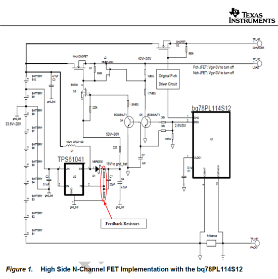
The use of N-channel MOSFETs enables a much better selection of very low Rds parts. It would obviously require a different driver design, but as far as I can see, there is no fundamental reasons why this should not work? It is used on TI battery AFEs like the bq29330.

Using MOSFETs with integrated current sensing would again reduce the number for available devices but reduces the power loss of the current current (!) sensor. This would either require low-side switching or current sensing level shifting to be compatible with the BQ78PL114 current sensor inputs.

Has anyone some inputs on one or both of these possible options?

  •  

    The selection of N-channel MOSFET with low Rds at acceptable prices seems to justify the added complexity caused by added circuitry.

    Here is suggested circuit for implementing a charge pump and driver in a SOT23-6 capsule. It requires only a few parts more than the bq78PL116 reference design. The suggestion make use of a new high voltage ideal diode driver from Nat.Semi that handles 75V (100V peak).

    It works by monitoring voltage on both sides of the FET via the IN and OUT terminal. It will turn on the gate when the IN pin is raised minimum 30 mV higher than OUT pin using a charge pump supplying 30uA gate current. The gate voltage is then raised until the IN and OUT levels are identical or until the gate voltage is clamped by an internal zener diode.

    If the IN pin voltage becomes 30 mV less than OUT pin the gate charge will be shorted to drain within 50-100ns using a built-in high current FET. This is controlled by the voltage divider R1/R4 (R7/R3) that feed OUT with a voltage around half battery voltage when DSC (CHG) is active and around 8V above IN when DSC (CHG) just becomes inactive.

    To save power the charge pump circuit is also turned off by lifting GND pin when the bq78PL116 DSC (CHG) signal is inactive.  

    I have not tested the circuit yet since the driver IC have just been released.  A possible killer could be that the IN or GATE pins get driven high when ground is lifted. That could be fixed by using an additional p-MOSFET to turn on VS when DSC (CHG) signal is active.

    I would appreciate feedback on this suggestion, good or bad.

    Per


  • Hi Per,


    The LM5050 is a High Side OR-ing FET Controller; this is not exactly what we need. We just need a High-Side N-Channel MOSFET Driver with a built in charge pump, such as the LM9061 (or just a charge pump?).

    The schematic is simple, see here:


  • The LM9061 has its drawbacks as well. It is certainly not a perfect match for the bq78PL116 power MOSFETs:

    1. It uses several mA (much more than the ML5050-1) even when off.
    2. It handles not more than 60V peak (ML5050-1 handles 100V) so it can not be used for 16S packs.
    3. It is in a bigger pysical package than the LM5050-1. 
    4. It automatically shuts down the MOSFET when voltage is above 26V.

    The best P-MOSFETs for 100V (16S with some margin) I have found have Rds=19mohm. For the same price I get N-MOSFET with Rds of 3.5mohm. Inclduing the loss in the body diode the P-channel version has almost four times as high loss at 30A requiring extra heat sink.

    Please TI, any good suggestions for a simple MOSFET driver with charge pump that can handle 100V and fit a bq78PL116 based BMS?


  • One with less than 500uA quiescent current draw!! :-)

  • 500uA is probably too much, I would prefer less than 10uA. The worst seems to be max voltage: 16 cells have typical max charge voltage of 67 volt so the driver should handle at least 70 V continously and 100 V peak minimum. Unfortunately N-channel MOSFET drivers suitable for bq78PL116 seems to be scarce if not non-existing as most high side MOSFET drivers that handle voltage above 70V are made for dynamic applications and lack independent charge-pump. These are the closest alternatives I have been able to find so far:

    • MAX1614 from Maxim has only 25uA max on current and 6uA max off current but is slow (gate current: charge 15-60uA, discharge 0.5-2 mA) and handles 26V max battery voltage.
    • LT1910 from Linear Tech. use max 2.5 mA in off state and 1.2mA in on state and handles 60V battery voltage.
    • LT1693- from Linear Tech. with two isolated drivers handles 100 V and seems at first quite nice except it lacks both charge pump and uses too much power.
    • LM9061 as described by Albert does not handle more than 60V and also use somewhat too much current.
    • LM5050-1 with GND pin lifted when turned off handles 75/100 V and has very low quiescent current consumption

     Does anyone know of other available IC driver alternatives?

  • Hi,

    We have a preliminary High Side NFET drive circuit that you can use. This is has a charge pump with adjustable voltage.

    See below. This circuit works well with the bq78PL114/116 because of the active balancing and hence all cells are kept equatable charged.

    You can start with Feedback Resistor values of 13.3Mohm and 162kohm

  • Yes, this circuit has been simultaed in SPICE. 

    The Vgs for driving the NFET is derived from the top cell, so it "rides" with the stack voltage to provide a constant gate drive.

    In addition, the TPS61041 consumes very low quescent current, and is a very cheap part.

    Would like to hear about your opinions and critics on it.

  • Thanks,

    This should work but is it not odd to discharge the battery unevenly by design? The primary purpose of a balancing BMS is to keep the cells balanced, not unbalanced?

    In addition, if the TPS61041 stops for some reason, then the datasheet says that VIN will be connected to SW so an extra transistor should be added to prevent shorting of the uppermost cell voltage as shown in the datasheet. A peek at app note SLVA136 shows an alternative way where they use another chip to supply 3.3V to VIN and EN from the same cell. But it all adds up the number of parts. Especially if the system, like mine, do heavy charge and discharge cycles thru the same wire - then the N-channel driver must be duplicated for the CHG signal so the number of required parts more than doubles compared to the LM5050-1 based suggestion (which unfortunately I don't know work or not).

    The best would be a simple and tiny charge pump that handles 100V, that would really be neat ;-)


  • The advantage of the bq78PL114 and bq78PL116 is that it utilizes the PowerPump (TM) Balancing algorithm (http://focus.ti.com/lit/an/slua524a/slua524a.pdf). This balancing methodology ensures that the cells are balanced up or down to main the cell voltage within 10mV of each other.

    The idea of this circuit is to minimize the number of components.

    Thanks for your suggestion on protection of the cells in case the TPS61041 stops working. We will take a look that.