This thread has been locked.

If you have a related question, please click the "Ask a related question" button in the top right corner. The newly created question will be automatically linked to this question.

EMC issus - UCD devices

Other Parts Discussed in Thread: UCD74120, UCD7242, UCD74106, TPS53513, LMZ31707, LM20333, TPS54521, TPS62177

It happened that during EMC pre-conformance session, we didn’t pass the radiated emission test.

We had some problems with spurious in low frequency range 30/230 MHz IEC 61000-6-3.

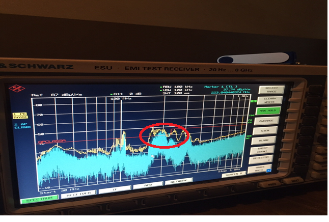
In particular we had some spurious around 200 MHz that exceed the limit.

In figure below a picture from EMI test receiver to give you the idea of what we get.

Please consider only the pick around 200 MHz, the others are due to the fact that the picture has been the with anechoic chamber open.


We have been able, with some difficulties and approximation, to reproduce the issues in our lab and at the end we can see a similar behavior also on our spectrum analyzer.

After some weeks of analysis we realized that the cause could be the TI DC/DC converters: UCD74106 (1x),  UCD74120 (2x) and UCD7242 (2x).

To demonstrate this we supplied TI TCI6638K2K with external power supplies and the spurious don’t appear.

After this, we switched on the UCD only with a load and the spurious came out again.


Another thigs that we note is that in UCD datasheet is written “Parasitic inductance in the high-side FET conduction path and the output capacitance (Coss) of the low side FET form a resonant circuit than can produce high frequency ( > 100MHz) ringing on this node.” It seems similar to our case.


What we basically did for AZCOM TCI6638K2K board design is to copy the supply scheme from TI evaluation board  EVMK2HX Evaluation Modules from Advantech ( http://www2.advantech.com/Support/TI-EVM/EVMK2HX.aspx ). Also BRD is pretty much the same.


Can you please support us and give us some inputs to proceed in our solving mission?

We would also share schematics, BRD and other data helpful for this analysis.


Thanks in  advance

  • Please check the ringing frequency at the SW nodes of UCD74xxx and see whether the ringing frequency matches the observed emission. You may disable individual UCD74xxx to find out which one causes the most emission.

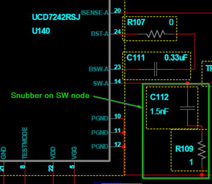
    Once the emission source is identified, you may add a snubber as show below. It will damp the ringing on the SW node.

    Also, please ask Advantech whether the EVM has passed EMC test if you are using the same layout.

    Regards,

    Zhiyuan

  • Hi,

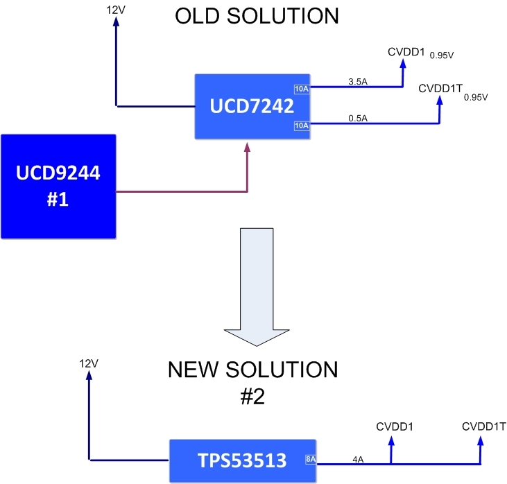
    We have noted that those spurious are generated mainly by the UCD7242 device that generates 0.95V (CVDDT1 rail 3 and CVDD1 rail 4). Reducing the frequency switching (from 751KHz to 300KHz) we have improved the EMC, but in order to pass the test session, we have to redesign the power distribution and avoid the use of UCD7242 device.

    Furthermore we have noted that the current consumption is much less than the UCD7242 capability.

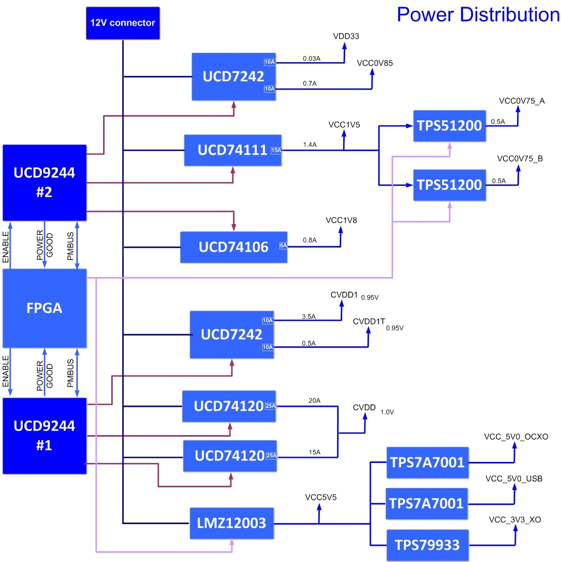
    Please note that the SoC power distribution is the same as Advantech EVM (EVMK2HX). In attach the block diagram.

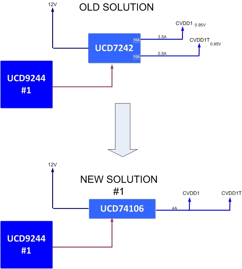
    Below  the solutions we want to implement for the generation of 0.95V @4.2A:

    1) Use of UCD74106 device. (This device is already used in our board to generate 1.8V):

    2) Use of TPS53513 device (394KHz frequency switching, 86% efficiency):

    3) Use of LMZ31707 (250 frequency switching, 86% efficiency):

    Which solution is better in terms of EMC? Are there any issues using one of these device instead of UCD7242?

    We want also to replace the other UCD7242 that we used for the generation of 3.3V and 0.85V. Also in this case, the current consumption is much less the maximum output current of UCD7242.

    For the generation of 0.85V @0.7A we could use:

    1) LM20333 (200kHz frequency switching, 78% efficiency)

    2) TPS54521 (495kHz frequency switching, 77% efficiency)

    For the generation of 3.3V@0.03A we could use:

    1) TPS62177 (242kHz frequency switching, 85% efficiency)

    2) TPS563210 (32kHz frequency switching, 90% efficiency, DCM mode)

    What your suggestions about the solutions proposed?

    We have used TI Webench to find the right device (frequency switching, efficiency, output current…)

    Thanks for your support.

    Regards,

    Simone

  • There is no EMC information available for UCD7xxx devices. Sorry. The EMC performance also heavily depends on the layout (e.g. distance between SW node and inductor, distance between input caps and UCD7xxx, etc.), so it is difficult to provide useful information. At 200MHz range, I think the emission source is the SW node ringing. Did you try the snubber? Placing input caps and inductor closer to the UCD7xxx with strong return path will also help.

    For EMC performance of other TPS devices, you may post questions to corresponding forums.

    Regards,
    Zhiyuan
  • I have tried the snubber, but I didn't see significant improvement...

    I have seen some improvements with a lower frequency switching. So my idea is to set the frequency switching of all device to 300 KHz (the minimun allowed). Are there some issues with using these devices with the minimum frequency switching?

     There is no way to know which devices (UCD or TPS)  are better in terms of EMC immunity?

    Thanks.

    BR

    Simone

  • By cutting the switching frequency in half you have reduced the switching losses of the converter, but you have doubled the ripple current in the inductor which will increase your conduction losses and the noise on the output voltage.  Care must be taken to ensure that the existing components can withstand the higher stress and the system can tolerate the increased noise.  You may need to adjust your component selection to account for the reduced frequency.

  • Reducing frequency will also have negative impact on transient response. Make sure the new frequency setting can meet the requirement.

    I think layout has big impact on EMI. Discussing device EM emission alone doesn't have much meaning.

    Regards,
    Zhiyuan