This thread has been locked.

If you have a related question, please click the "Ask a related question" button in the top right corner. The newly created question will be automatically linked to this question.

TIDA-00173 Problem

Other Parts Discussed in Thread: TIDA-00173, UCC28711

I assambeled TIDA-00173  board but  the  CDD is not charged  I try to   disconnect  D29  , Q25  and  connected separate power supply with 24V  to see gate drive pulse for (initiate three small gate drive pulses) but it didnt happen :( . i think NTC pin when is disconect it should have 5 v But sadly It does not have any voltage on it .

so how should I know if UC28711 is fine ? is it enough to conect VDD= 24 volt, NTC disconected, GND =0 volt(GND) , HV disconected,CS disconected,DRV for test conected to scop to seeinitiate three small gate drive pulses?

Please Help me to solve it thanks :)

thanks for attention


  • Hamid,
    Can you provide some waveforms of DRV, VDD, and Q2 drain(switchnode) of your testing? Please also include what Input voltage and output current you are using? I'm assuming this is startup situation or it fails like this after you had it working?
    Regards,
    John
  • dear John thanks for repling.
    in fact it doesn't have any singal in DRV,VDD :(
    my current on HV pin is high enough (300uA ,110VDC) to start up VDD capacitor but VDD have zero voltage and never charged .i tried by several UC28711 but sadly it did not work.
    How can I test my UC28711 to see if they are fine ?
    dear by texting is to hard too describe all of factors and parameters ,I would be happy if you help me since I really need it ,so do you have whatsapp or any other online apps to contact to solve my problem .
    thanks in advance.

  • Hello Hamid,

    Since you say that the VDD capacitor never charged, I suggest that you inspect the capacitors on VDD and look for a short-to-GND. There may be a solder ball or an internally-shorted capacitor (see C32; ceramic caps can crack and short) that keeps VDD low and prevents start-up.

    When you applied external +24V, did you notice if there was 24V at VDD, or if the external source became current limited and stayed at 0V?

    Assuming that any short on VDD is removed, when checking the UCC28711, do not disconnect CS or DRV. These signals must be connected in order to see the 3 small pulses at start-up.
    You can apply some voltage to the board's DC input starting from 0V and slowly increasing it. When Vin is high enough to turn on the internal HV start-up FET and VDD starts rising, you may see only one output pulse at DRV. Normally, DRV is turned off when the voltage at CS reaches the CS threshold, which will be Vcst(min) = 0.195V at start-up. If input V is too low, the CS voltage may not reach this threshold before an internal cycle timeout triggers an open-pin fault and start-up is aborted.
    As Vin is raised further, eventually the CS signal can reach the threshold before the open-pin time-out and the three short start-up pulses will be seen. These 3-pulses will still cycle through UVLO on and off, because Vin has not reached the Run threshold (set by R27 and T1 pri-aux turns-ratio), but this cycling indicates that the UCC28711 is working correctly. None of this can happen, of course, if VDD cannot charge above 0V, so this issue must be cleared up first.

    Regards,
    Ulrich
  • Hello dear Ulrich thank you for time trying to solve my problem and again thank you for repling very fast :)

    I test my board to see if is there any short circuit exist i treid to connect 30v to VDD as you said furtunatly isn't any short circuit .

    but it did not worked :(.

    Dear , I want to go step by step to test my UC28711 .so

    I want to test my circuit in safe voltage as you know 400 v is so dangruse

    1.would you please tell me the lowest voltage to oprate Start-up?
    would it be fine if I connect to HV pin to 30V 300uA

    information of my board is
    (VDD=30V(external supply),VS=like TIDA-00173 (I did not connect HV 400V to DCBus), NTC= N.C,GND=GND,CS=Connected to R0.91ohm).

    2.if I leave HV disconnect(N.C) and then apply voltage to VDD(30v) and DRV connected to Mosfet gate , should i see 3 plulse in DRV?

    4. would it be ok is I leave NTC pin disconect? for start up test ?

    dear would you please tell me if is there any way to have online chat to send the picture form what I have done(like email whatspp or etc... )?

    Please help me to sove my problem .
    thanks inadvance .

  • Hello Hamid,

    I'm sorry I am unable to conduct a chat session or use Whatsapp. You can attach files to your E2E posts by clicking on the "Use rich formatting" button located at the bottom-right of the post window. Use the paperclip icon on the formatting toolbar to insert a file into your text.

    About testing: I agree you should use voltages less than 100V to debug this board. HV starts to conduct current at around 30V, but it may not be the full start-up current as specified at 100V. However, it should be enough to make VDD rise if there is no external short to GND on VDD.
    I am confused. In your earlier reply to John, you said the VDD has zero volts and never charged, even with 110Vdc on HV. But in your latest reply to me, you had applied 30V to VDD and there is no short. I don't quite understand the conditions of your testing, but in the long run, the TIDA board should start-up from HV, so I recommend to power up VDD by applying voltage to HV and let the IC control the operation.

    1. Open NTC pin (remove Q5). Open HV series resistors (remove R47).
    2. Remove all power sources from the main AC and DC inputs. Apply 30~50Vdc to HV_START (cathode of D13) and observe VDD. VDD voltage should cycle up and down between ~21V and ~8V over the course of a few seconds. You may have to slow down the scope sweep speed to 1sec/div to see it.
    If this does not happen, there is no point to look for anything else. VDD must go up and down that way before looking for any pulses.
    3. If VDD is stuck at GND with the UCC28711 in place, remove the IC and see if the VDD cap can be charged to ~30V with no load on it. If yes, that UCC28711 may have been damaged somehow, then try another one. If no, you have to debug the VDD network on the board first without the IC in place.
    4. When you do see the up/down zigzag of VDD voltage at step 2 (with IC installed), then look for a single output pulse on DRV at each peak of VDD. In this test condition, it will only be one pulse, not 3. When you see that, you can add a source to the main DC input and start to raise its voltage. At some high-enough voltage, the CS signal will reach ~0.2V within the open-pin timeout limit and it will switch to 3 pulses. It still won't start-up, but you'll see the three DRV pulses repeating at each VDD peak. The whole converter should start up when Vin reaches the Run threshold programmed by R27 and the transformer turns-ratio, but I don't know what that is for this TIDA design.

    I hope this debug procedure helps you to get the board running. Basically: keep simplifying a larger network into independent, smaller, simpler networks and verify that each simpler network works as expected before recombining to more complicated ones. This includes removing parts or connections to isolate between sub-nets. This way you can uncover a problem which interferes with the operation of other sub-networks.

    Regards,
    Ulrich
  • Hi dear Ulrich

    you have spent alot of time trying to help me  thanks for that!

    from that part that you told me that you got confuse ,I would say that I test my board either 30 v or 110v (both).

    the things that i reailzed is I dont have problem (short circuit) in my board I removed UC28711 and conected HV(50v) to VDD and capcitor was chaeged :),I realized that my UC28711 got dameged I tried by 3 other UC28711 which I used it before it did not work :(

    I think all of my UCC28711 got damaged I have to buy them again form china ,it tooks 20 ~30 days to have  them. as soon as I get I will tell you about it ..this IC really disappointed me :(

    thanks for your help again dear .

    best wishes.

    Hamid.  

  • Hello Hamid,

    I'm sorry for my delayed reply, and also sorry for your bad experience trying to use this part. The UCC28711 and its related family controllers have been successfully used in hundreds of applications with millions of parts. I can only think that the components you tried had become damaged (VDD input short to GND) in some systematic way.

    To try to account for this (without casting blame one way or the other), consider these possibilities:
    a. parts were already bad from the vendor;
    b. parts suffered from ESD (electro-static discharge) during handling before or during being soldered to the board;
    c. +24V or +30V test voltage source overshoots above VDD absolute-maximum rating when switched on, before coming to regulation;
    d. applying VDD test voltage through long wires allows stray lead inductance to ring VDD voltage up to 2 x Vsource, which over-stresses VDD;
    e. some unknown circuit path on the pcb allows HV voltage to directly or indirectly connect to VDD, resulting in overstress.

    Please investigate each of these possibilities to avoid damaging your new replacement parts.

    You can also request a sample of the part from the UCC28711 product folder on the TI website, and/or contact a TI sales representative in your local area to request some samples. Maybe they can deliver faster than your original source.
    I hope the new parts will work the way you expect them to.

    Regards,
    Ulrich

  • hi dear Ulrich

    How is it going?

    First of all I want to thank you for accurate response ,it was absulotly helpful :).Thanks a million!

    I have bought a new UC28711 and fowllowed your instruction step by step . I could see up and down zig zag voltage

    at VDD (pin1 of UC28711) & one pulse on DRV , then I tried to increase the voltage of DC bus to 230VDC and I saw 3 pulse in gate drive :).

    but sadly I could not stable PWM signal , it just applies 3 pulses to gate of mosfet and DRV becomes zero . over cuorse of few second and reppite this cycle again.

    as you mentioned before:
    "Basically: keep simplifying a larger network into independent, smaller, simpler networks and verify that each

    simpler network works as expected before recombining to more complicated ones. "

    so my project got like this :

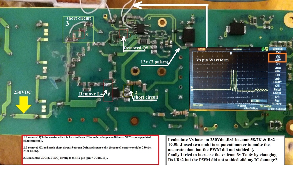
    1. I removed Q5 (the mosfet which is for shutdown IC in under-voltage condition so NTC is unpopulated

    (disconnected)).

    2. I removed Q1 and made short circuit between drain and source of it (because I want to work by 230vdc,

    NOT1200v).

    3.I connected VDC(230VDC) dierctly to the HV pin (pin 7 UC28711) .


    4.during 3 initialize pulses I measured VFB by oscilloscope . It was 13.2v on each of impulse.so I conclude  that
     primary-to-auxiliary turns ratio would be 17.4 (230 VDC /13v =18 ).

      4.2  RS1=Vin(Run) / N(PA) x I VSL(RUN)   =>  RS1=230VDC / (18 x 225uA) = 58.7 k

      4.3  RS2=(RS1 x 4.05v )/ (0.66+24.6)+4.05  => RS2=(58.7 k x 4.05v )/ (0.66 x 24.6)-4.05 =19.5 k


    5.I calculate Vs base on 230Vdc ,Rs1 became 58.7K & Rs2 = 19.5k .I used two multi turn potentiometers to make the accurate ohm. but the PWM did not stabled :(.
    finally I tried to increase the vs from 3v To 6v  by changing two multi turn potentiometers (Rs1,Rs2) ,but the PWM

    did not stabled .did my IC get damage?

  • Hamid,

    Thanks for your follow up. Ulrich is traveling presently so please expect some delay until early-mid next week.

    If you need a response sooner than that I can try to get someone updated on the history here.

    Regards

    John

  • thanks dear Johon for your attention .
    ya , I need a response sooner, I would be happy if some one else ansewer me.
    if I could not solve my issue then I wait for Uirich to come back from his travel.
    Best Wishes.

    -Hamid
  • Hello Hamid,

    I'm sorry for my delayed reply.  For step 1, removing Q5 is a good step. Steps 2 and 3 are also good.  I recommend that you start with a lower dc input voltage for troubleshooting.

    At step 4. I see a problem with the VFB waveform: it looks to be upside down.  In other words, the waveform is inverted.  When Q1 is on, the voltage at VFB should be negative with respect to PGND, not positive.

    I suspect that the auxiliary winding is connected in backwards polarity.  Please reverse the connections at T1-pins 6&7.  Then make sure that VFB is negative when Q1 is on.  With low input voltage (say ~50Vdc) VFB should be only about -3V.  There may be only one pulse at this low input.  As you raise input voltage VFB should also increase and at some point you will see 3 pulses. 

    With RS1 = 58.7K, the controller should start to run at about 230Vdc on the input as you calculated.  If you reduce RS1 and RS2 each by the same factor (say x 0.5 or x0.25) you can see it try to start up at lower input.   It may only switch for a short time because there may not be enough output voltage to sustain the auxiliary bias voltage (VDD of UCC28711), but it should switch many more times than 3 pulses and then repeat as VDD goes up and down through the UVLO cycle.

    At some higher input voltage, Vout should get high enough to keep VDD above UVLO and the device should stay switching. 

    Please check the Aux winding connections for proper polarity.

    regards,
    Ulrich


  • hi dear Ulrich
    Good day!

    at first .I want to thank you for helping me :).

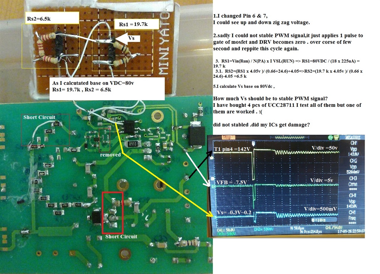
    I changed pin 6&7 of T1 ,as you mentioned. but still the stability issue is not solved :(.

    please bear with me , and help me ,thanks.

    I don't know why is that...

    I change 3 UCC28711 but the response of all of them are the same!

    did my ICs get damage?
    or I did some thing wrong!

    please kindly take a look at the picture .

    Best wishes.

    -Hamid.

  • hi dear Ulrich
    Good day!

    at first .I want to thank you for helping me :).

    I changed pin 6&7 of T1 ,as you mentioned. but still the stability issue is not solved :(.

    please bear with me , and help me ,thanks.

    I don't know why is that...

    I change 3 UCC28711 but the response of all of them are the same!

    did my ICs get damage?
    or did I some thing wrong?!

    please kindly take a look at the picture .

    Best wishes.

    -Hamid.

  • Hello Hamid,

    I apologize again for my delayed response; I have been very busy catching up from my travel.

    Changing pins 6&7 of T1 was the right thing to do.  The new waveforms look correct now, instead of inverted. Please do not consider the 3-pulse issue to be a stability issue.  It is an operating mode issue and the first three pulses are in the start-up mode and if operation stops after 3 pulses, it means that the IC is detecting some kind of fault condition.  In the fault mode, it stops switching and cycles VDD back to start-up over and over until the fault condition goes away.
    All four ICs that you tested are operating correctly.  Now we need to find out what the fault condition is that prevents further switching to get out of the Start-up mode and into the Run mode. 

    In the waveforms above, we see 142V peak-peak on the switching node.  This comes from ~130Vdc bulk voltage during the on-time plus ~12V reflected voltage from the secondary during the demagnetization time.  VFB shows -7.5V during the on-time.  VS = -0.25V during the on-time, because there is an internal clamp at ~0.25V below GND when current is pulled out of VS through Rs1 when VFB is negative.  (-7.5V - (-0.25V) / 20K = 363uA which is > 225uA for start-up, so "low input voltage" is not the fault condition which prevents start-up.  Certainly, output overvoltage is also not the fault in this case. 

    The fact that you have only a single pulse at start-up instead of 3 is an important clue.  This situation can happen when there is no signal at the CS input.
    You can see that the on-time of the single pulse appears to be ~12us on the 50us/div time-sweep scale.  The UCC28711 has this 12-us time out for maximum on-time at start up.  The control requires to see a signal at CS input that exceeds the Vcst(min) level (= 0.195V) within 12 us or it stops switching after 1 pulse.

    Please check to make sure that a ramping signal going up to 0.195V appears at the CS pin.  Probe directly, but lightly (don't push down hard), on the pin to ensure that the pin is soldered correctly to the board.  There may be two possible problems here:
    a.  there is a disconnect somewhere and CS input is open, or
    b.  the inductance of the primary winding is so high that the CS signal is ramping but cannot reach +0.195V even after 12us of on-time.

    I don't know what the inductance of T1 is for this TIDA design, but because this is a high voltage design starting up at a very low input, so I think that "b." is most likely to be the cause of this "fault".  If so, the one solution (without changing anything else) is to increase Vin until Vcs reaches 0.195V within 12us. Another solution is to (temporarily, for test purpose only) increase the value of the current sense resistor R22 by doubling it or higher.  This will give a larger signal at CS, but it also limits the available output power to 1/2 or lower of the normal rating.  For test and debug, this should be okay until normal running is established.

    Please check the CS signal and proceed as discussed above. Also, please look at Section 8.3.2 of the UCC28711 datasheet for a description of the fault protection built into the IC, which could affect start-up. 

    Regards,
    Ulrich

  • Hi dear Ulrich.

    How are you doing ?

    First of all I appreciate for spending time and effort to solve my problem.Thanks :)
    Your description is just like an algorithm which is perfect!
    Believe it or not, It made an impression on my lifestyle to be more organized and sequential.


    Your guess was true. the problem was from R22 ( section(b) ),which needs to be quintupled ,So I insert 5 ohm.it was 0.91 ohm at first.
    In 5 ohm for R22 and 210 VDC_link , the voltage of CS can reach to 0.200v which is >0.195v. so I could see four pulses. but after that it stops . :(

    Some thing that confused me is that, VFB =-7.5 ~ -14V is nagetive (as shown in oscilloscope) which can not pass into D28 ,D29 In other words, these diodes are in reverse-bias! .

    And also positive part of VFB is too small ,around 1 volt (by 210 VDC_link ) as you can see in the picture. which can not effect on D28 ,D29.

    So I could not figure out how the Auxiliary coil can power-up IC to make it stable.

    I was wondering if you tell me how I can stable the power supply switching?
    I would be happy if you help me to solve all of problems.

    Best wishes.
    -Hamid.


  • Hello Hamid,

    I’m sorry for my late reply; I haven’t forgotten about you, I've just been very busy. I’ll try to get you past the 4 pulses to normal running… it looks like we’re almost there.

    First let me explain how the start-up should work. When high voltage is applied to pin 8 (HV) of the UCC28711, the IC will connect an internal current-limiting FET to VDD and pass current to charge up the VDD capacitors C10 and C32. For the IC to start-up and run, VDD must charge to 21V. At this point, D29 and D28 are reverse-biased, C11 has no charge, and the IC starts to switch with 3 short on-time test pulses. If the IC detects no faults during these three pulses, it continues to switch with wider on-time to charge the outputs. Energy stored in the transformer inductance during the switch on-time is delivered to the outputs during the demagnetization time. During the 3 test pulses, this energy is very small, so little charge is sent to the outputs, but even so, this energy (current pulse) flows through the output diodes to the output capacitors. The caps may be at zero volts but the diode has a finite diode drop and this drop is reflected back to the primary winding during the demagnetization time. You can see this in the waveform as ~0.5V level for ~150us after the first on pulse. In the next 2 pulses, the reflected voltage increases slightly and the demag time decreases as a little voltage is building up in the output caps. In the 4th pulse, the longer on-time yields a higher peak current which raises the output voltage more, so the demag time become longer again. Unfortunately, something was detected during this pulse or this plus the previous two pulses that caused the IC to believe that there was a fault and shut down. If the pulses had continued, output voltage would continue to build up and reflect higher and higher voltage at the auxiliary winding during the demag time.

    The aux winding has two duties: to serve as a bias supply for the controller and to serve as a sense winding for the reflected voltage. During the demag time, the aux winding voltage is a reflected and scaled version of the output voltage, so the controller can regulate the output by sensing this winding with the VS input. Please refer to the datasheet for full details on how this works. In addition to providing a sense voltage, the aux winding also delivers charge to the aux caps C11, C10 and C32 through diodes D28 and D29. Because this happens during the demag time, the output voltage must be high enough to reflect enough voltage at the aux winding (by the sec-to-aux turns ratio) to keep the VAUX bias voltage above the UVLO turn-off threshold of the IC. This threshold is ~8V and the turns ratio from 24V to VFB is 3:2. Therefore, the 24V output voltage must increase to at least 12.5V to keep VDD from falling below the 8V turn-off threshold, or the IC will shut down and restart. During the time that Vout is less than 12.5V, the IC and MOSFET gate drive is running entirely on the charge stored in caps C10 and C32, starting at 21V and draining down toward 8V.

    During this start-up, D29 will be reverse biased, but the small reflected voltage at VFB will forward bias D28 and C11 will start to charge up along with the other outputs. Once the voltage on the main outputs is high enough, the voltage on C11 will also be high enough to forward bias D29 during the demag time and keep VDD above the UVLO threshold.

    Now the problem is to understand why the IC shut off after the 4th pulse. At this time, I’d like to review the changes that we have made to the board to bring it to this point. The TIDA-00173 is intended to be a high-voltage input converter and we have modified it to try to run at low voltage for easier and safer debug. We’ve changed the VS resistors and current sense to try to scale it down. I don’t think the problem is input undervoltage (brownout) since the DC link is at 210V. I don’t think it is over-temp because pin 3 is open. I don’t think it is a VS pin fault (open or short to GND). That leaves possible overcurrent at CS or output OV. The R-C filter at CS input is heavier than usual and causes a 680-ns sensing delay at the CS input, but since the R22 resistor has been changed to 5ohm the peak current is much lower than normal. It is difficult to imagine that the voltage at CS can rise to 1.5V and cause a shut down. That leaves output OV detected at the VS input.

    Now, your CH2 waveform is at VFB, and the voltage at VS is ~¼ of VFB, so detecting output OV at 4 pulses into the start-up seems unrealistic. But your photo shows that the VS divider resistors are on a daughter board mounted beside the main board, with long wires attaching to the IC. VS is a sensitive input and these wires may be picking up noise that is not visible at VFB, but affect the sensing as VS and cause it to malfunction, or falsely detect a fault. Please remove the daughter board and place the VS resistors on the main board pads. If you can find SMD parts, please use them. If axial parts are the only ones available, please minimize their lead lengths and try to use only one part for each position, if possible.

    If this change results in a long series of pulses, but still shuts down after a while, don’t despair. Once you get the long series with the existing modifications, we can back out the changes one by one to get back to the original circuit.

    Regards,
    Ulrich
  • Dear Hamid, Ulrich, John,

    I am also in the process of designing an SMPS based on the details provided in TIDA-00173.

    I have a question regarding the NTC pin of this IC UCC28711. I do not want to to use the protection function provided by the NTC input. So in my final circuit, should I connect a high value resistor to it or keep it open (i.e. not connected to any resistance)?

    The way I understand it is that this pin is a current source with 105uA (typically) coming out of it. And if I were to connect a resistor from NTC to ground of say 30K, then the current source will bring the voltage on this pin to 30000*105*10^-6=3.15V, which is well above the shutdown threshold of 0.95 V (as stated in the datasheet).

    Is this analysis correct and will the IC work fine without going into fault turn-off using 30K resitor to ground on NTC pin?

  • Hello Ahsan,

    Your analysis is correct. You can add the high value (30K or higher) to GND, or simply leave the NTC pin open, if you don't need the protection function. The IC will work fine in either case.

    Regards,
    Ulrich
  • Hi Ulrich,

    After reading your suggestions in the entire thread, I have designed a circuit as follows:-

    I have left NTC pin open, Connected HV to the input bulk capacitor, connected Rcs= 2.2ohm with RLC=1K compensation resistor, Gate drive resistor is 10 ohm.

    I am using the same transformer as used in  tida-00173 application note and the resistor network connected to VS is also the same as detailed in the application note. 

    Results:-

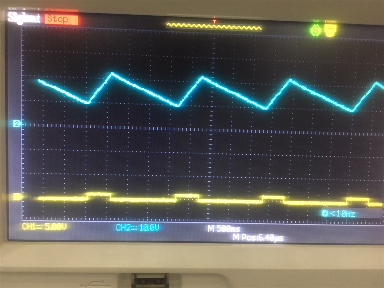
    The Vdd pin charges upto 21V and then gets discharged down to 8V and this is repeated continuously.

    Initially I started getting single gate drive pulses periodically when I gave input voltage around 390VDC (which is the maximum available in our lab). But then after reducing the values of the resistor network on Vs pin to rs1=75K and rs2=25K, I started getting 3 gate drive pulses. I guess this was because of the fact that the Vs pin was not getting the 225uA it needed to start operating and the IC went into input bulk undervoltage fault reset. 

    During this time I probed the NTC pin and it showed strange behaviour, showing 5V pulses at random intervals. 

    And after a while the 3 gate drive pulses stopped and DRV pin started showing square pulses of around 1V. Kindly give some input regarding this issue. 

    I am attaching a screenshot of the oscilloscope: the blue channel shows VDD pin and the yellow channel shows gate drive pulses.


  • Dear Ulrich,

    This is the output that I am getting. The blue channel shows, VDD and the yellow channel shows gate drive pulses.

    I have used RS1=75K, Rs2=25K, Gate drive resistor=10 ohm, current sense resistor=2.2 ohm, transformer is the same as the one used in the TIDA. Hv is directly connected to the 390V input bulk capacitor (which is the maximum available in our lab) and NTC pin open.

    Initially, I was getting 3 gate drive pulses but suddenly it stopped and the attached waveform started happening. 

    The NTC pin also showed 5V pulses at random instead of being stable at 5V.

    PS. @ I do not wish to hijack your post. Just hope that we can learn from each other's mistakes and experiences and make it easier on ULRICH to explain things in the same post. 

  • Hello Ahsan,

    The waveform you show for DRV output is definitely abnormal. There should never be 1V during the VDD charge-up time. The UVLO turn-off and turn-on thresholds also appear to be shifted higher than normal. And NTC should not have random pulses on it, but should be a continuous ~5V after start-up.

    I believe this IC is damaged and should be replaced. I am concerned that the replacement may also fail if the root cause of the previous failure is not discovered and corrected. You had observed the normal three test pulses for start-up, but then they stopped, with the resulting waveform shown. This tells me that there is some overstress on one of the pins (it could be more, but probably only one) during the initial turn-on attempts and the IC apparently survives this stress for a short time but then fails.

    Let's look at the clues available:
    - VDD rises ~12V in 500ms. Cvdd = ~11uF, so Icharge = 264uA, which is normal. So the HV and VDD pins are working.
    - NTC is open, so that shouldn't be a problem.
    - ~1V on DRV while VDD rises. Well, if Q2 G-S were shorted, it would imply 100mA output, but that can't happen with only 264uA input during charge up, so I think DRV is simply reflecting an internal offset during charge up.
    - If the GND pin was open, CS might become the next available "GND" for the IC, but 1V across 1K = 1mA, and this is still 4X higher than the charge-up current (so VDD couldn't rise). but we don't know what things looked like before the failure.
    - Only VS is left, and 75K with 25K are reasonable values.

    To be honest, I don't have a good idea, but would suggest to check several things:
    a) check to make sure GND pin is well soldered to the pcb and the primary GND network is continuous everywhere.
    b) check the 75K resistor on VS to make sure it is the correct value (not 7.5K or some wrong value).
    c) check the DRV and CS waveforms and drain voltage on Q2 during the three start-up pulses (with new IC)
    d) make sure that you use an isolated input AC (or DC) source, or do not connect scope probes to primary side and secondary side at the same time. The short-circuit path through the scope gnd will cause a high stress somewhere, when a non-isolated source with a limited impedance is used. Usually the fuse blows, or the diode bridge fails, but other strange things could happen.

    regards,
    Ulrich
  • Hi Ulrich,

    I have managed to make the power supply work properly. I am drawing 1.5 A at 24V from the isolated 24V output between pins 14 and 12 of the transformer and it is working fine. 

    I have a question regarding the optional Vaux supply being derived from the VFB. My application actually requires:-

    1) An isolated 24V supply with 600-700mA current capability which I AM deriving from the output between pins 12 and 14 of the transformer as stated above.

    2) a non-isolated 24V output (referenced to PGND) with 600-700mA current capability which I PLAN to derive from the optional Vaux output of the power supply. 

    Since Vaux is being driven from VFB and VFB also gives supply to the VDD capacitor and feedback to the VS input of the IC, will using Vaux (driving 600-700mA current out of it) in any way effect this feedback and Cvdd voltage?

    Secondly,

    The TIDA states that in order to derive output from Vaux output, the 24V isolated supply power should be derated accordingly. What does DERATED really constitute and how much derating is required? 

    1) Do I need to change the values of components like e.g. the value of Rsense resistor to reduce the power output of the 24V supply to be able to drive power from Vaux?

    2) OR I do not change any component values and just reduce the external load at the isolated 24V output?   

  • Correction to the above:-

    The Vaux output is 16V and I plan to use a boost convertor to boost it to 24V.
  • Hi Ulrich,

    Any update regarding my post?