This thread has been locked.

If you have a related question, please click the "Ask a related question" button in the top right corner. The newly created question will be automatically linked to this question.

UCC28050: How the UCC28050 knows when it should turn on and off its power switch?

Part Number: UCC28050

Dear team,

My name is Oliver Kim, TI Korea FAE working in HKMC account.

When I looked into UCC28050, I couldn't understand how the power switch is turned on and off?

I believe,

phase 1) power switch turns off when switch current becomes inductor current peak envelope.

phase 2) power switch turns on when diode current becomes zero

as shown in fig b) TM control

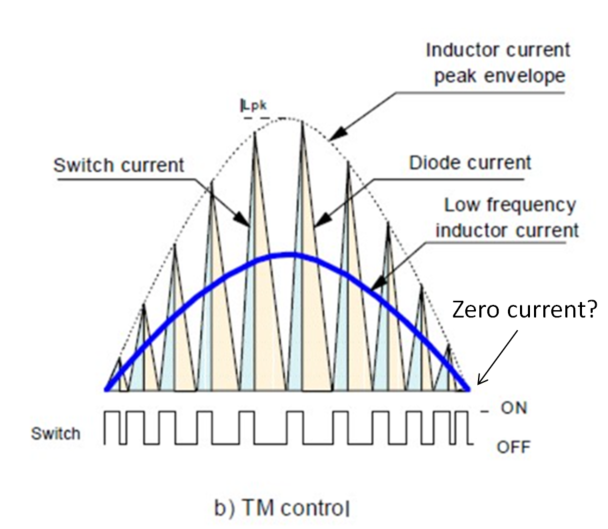
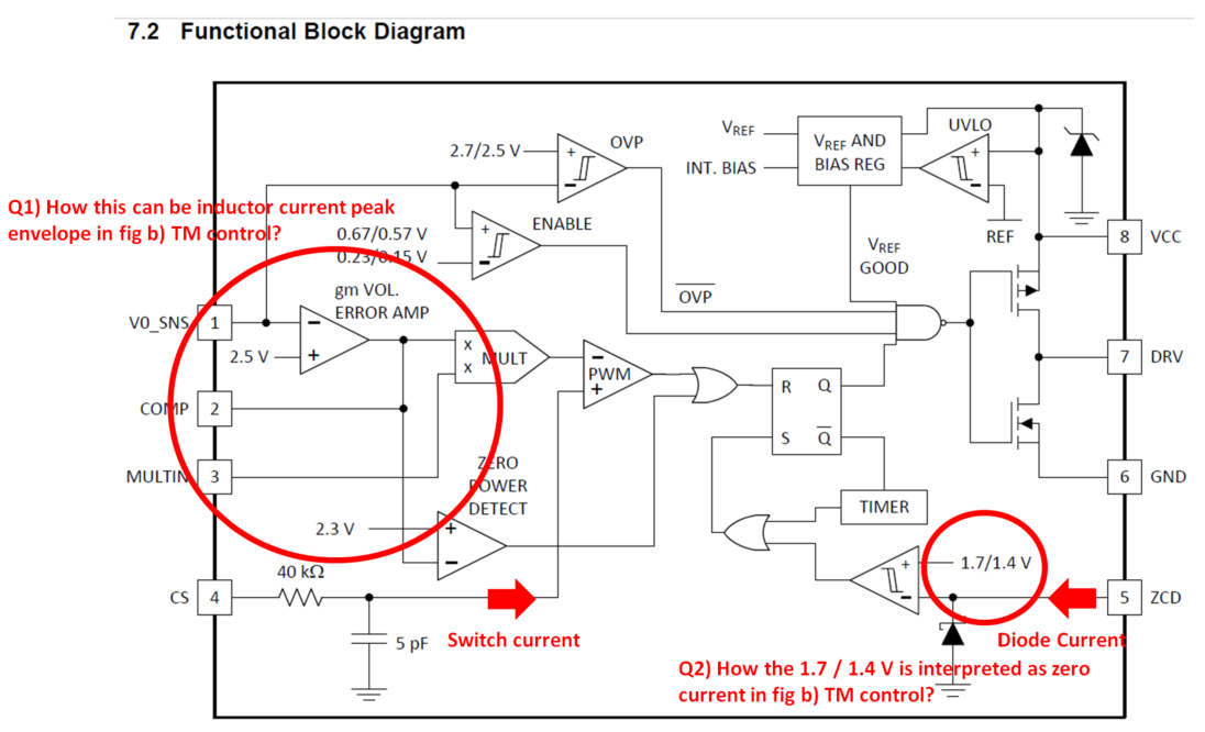
We can detect switch current by CS pin in UCC28050, but how inductor current peak envelope can be detected? (Question 1)

and also, we can detect diode current by ZCD pin in UCC28050, but how zero current can be detected? (Question 2)

Thank you.

Regards,

Oliver

  • Hi Oliver,

    Thanks for your interest in UCC28050. The controller is looking at the line voltage through its MULTIN pin. The MULTIN voltage is then fed to a multiplier. The output of the multiplier is compared to the CS pin waveform to determine when to turn on and off the MOSFET. Becuase the inverting input of the PWM comparator is a function of the instantaneous line voltage, the on time of the MOSFET is a function of the instantaneous line voltage. This makes the on time longer when the rectified line voltage is at its peak and makes the on time shorter when the rectified line voltage is near zero. This also makes the shape of the input current follow the rectified line voltage.

    For critical conduction mode, the converter operates on the boundary between DCM and CCM. As such, the inductor current will momentarily fall to 0 during each switching period.

    The controller is able to sense when the inductor current has fallen to 0 through the ZCD winding. This is becuase when the inductor current hits 0 the MOSFET drain voltage drops. Section 7.3.3 of the UCC28050 datasheet discusses this in further detail:www.ti.com/.../ucc38051.pdf.

    Best Regards,
    Ben Lough
  • Der Ben Lough,

    Thanks for your kind explanation.

    But what I am really wondering is... why the output voltage goes into multiplier with MULTIN pin?

    Based on what you said, it seems that output voltage(VO_SNS) is unnecessary to turn on and off the MOSFET. (but MULTIN is needed)
     
    Of course, I read the datasheet but it was not clear for me.

    Could you explain how the VO_SNS and MULTIN interact in the multiplier?

    Thank you.

    Regards,
    Oliver

  • Hi Oliver,

    The output of the error amplifier is included in order to maintain output voltage regulation. The output of the multiplier is a function of the sensed line voltage and the sensed output voltage. As an example, this allows the converter to recover from a sudden increase in load current because the duty cycle is dependent on the sensed output voltage.

    The output of the multiplier is approximately equal to 0.67*Vmultin*(Vcomp-2.5)

    Best Regards,

    Ben Lough

  • Dear Ben Lough,

    Well, The 0.67*Vmultin*(Vcomp-2.5) seems to be the output of the multiplier, not the error amplifier.

    I really appreciate you.

    I am clear now.

    Regards,

    Oliver

  • Apologies, you are correct. The equation I posted is for the output of the multiplier, not the output of the error amplifier.

    -Ben