This thread has been locked.

If you have a related question, please click the "Ask a related question" button in the top right corner. The newly created question will be automatically linked to this question.

UCC27714: HS has phantom jump to HO

Guru 54088 points
Part Number: UCC27714
Other Parts Discussed in Thread: TIDA-00778

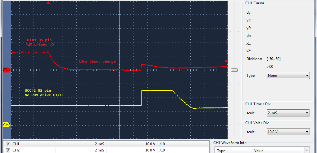
Finally seeing a pattern where one UCC Cboot charge cycle causes another static but enabled UCC HO output to suddenly go active without HI input triggering it.

The CH1 - HS of 1st UCC as LO pin receives 13ms PWM @50us periods to charge Cboot. CH2 - HS of  2nd UCC sits quietly but EN is logic high 3.0v and the 3rd UCC is effecting in the same way.

The HS pins of all UCC feed the MCU ADC channels as with other vendors gate drivers same basic circuit. We never see this issue in past but fight for weeks to stop this insane behavior even taking unusual steps in software to control Cboot charging cycles can not rectify this hardware failure. The only UCC not being much effected it the first Cboot charge or maybe even with delay added get the second to charge but the 3rd then jumps HO up like crazy. Surely TI tested UCC in three phase commutation high impedance ADC channels monitoring HS does not effect HO drive?

How is the 2nd/3rd UCC HO pin being trigged active state when no signal is input to HI or LO and VDD is highly filtered?


  • Notice how CH1 Cboot finishes LO charging near 13ms as Ch2 HO output suddenly goes active. CH2 HO without any MCU driven PWM on HI/LI jumps up to 24v supply rail of high side NFET then shuts off like nothing happened.

    Are these IC defective or others that produce a HO drive signal without input drive on HI/LI?
  • Hello BP101,

    That is very odd indeed. I also notice your HS nodes all sit around 14V at start-up. How does that voltage appear on the HS node?

    I doubt very much you have bad devices, we 100% screen every UCC27714 before we ship it out the door.
  • Hi Don,

    Floating HS is typical for 3 phase motor commutation, often far less around 10.5v float. Perhaps what is not industry typical (Fig 47) <100ns pulse restriction or seemingly LI setup time Not shown in (Fig1). The problem seems to be LI input will not handle 20khz PWM 50us pulses for pulling down Cboot without leading to HO output errata. HO jump seems is self inflicted by the driver behavior when LI is sent 20Khz PWM 1% duty cycle near 125ns pulses.

    With work around mention below, 8-80Khz Cboot charging does now succeed. 

    Part of the work around was mention by John in another post and required software rewrite, adding delay between sending (on/off) PWM out to LI in 333Hz cycles. That was no easy task besides totally unexpected behavior and touchy HS/HO issue remains even with that being done. The fight in my mind being, why would any different behavior of Cboot discharge than other vendors gate driver. I remain astonished how this Cboot issue flew under the radar in TIDA-00778. Seemingly they only tested AC motor drive sinusoidal wave forms in evaluation of UCC27714 gate driver. No warnings about other wave forms or PWM causing this LO input errata of HO.

  • Hi Don,

    Now understand  <100ns HI/LI blocking seemingly is causing issues with HO driven NFET slow decay mode.  Typically the pulse width of LO is set 1% duty <100ns widths, current circulates high side FETS and slowly decays as HO pulse width is typically much wider, roughly 20-30us in a 50us period.

    Adjusting the pulse width >100ns 2us or so fails to saturate the LO side FETS gate region and very little pulse width develops in any of the pulses. Some how high voltage is being created in the HO driven UCC of the second and third gate drivers but not the first. So 24vdc boosts 90-180vdc if we don't stop by software MCU safety fault checks.

    How is it possible to create such high voltage pulses and why do 1- 5us pulses appear very pointy, e,g, VVV? Most all the pulses being produced are very pointy, even zoomed in captures except for 50% duty then LO/HO pulses appear very square. It would seem the 50ns delay matching is not working correctly when two different pulse widths are presented to HI/LI and pulse widths are being shortened on both sides.

  • Some of the issues mentioned with Cboot charging slow fall was caused by a blown 15 amp Bus fuse inverter bridge 24v supply. ADC kept reporting 24vdc BusVoltage in GUI digital readout, must have come from +15 VDD leaking into 680uf bus filter cap.
  • It seems LO is disrupting HS during Cboot charging in the PWM cycles as there is no Cboot RC slope in HO turn on being immediate in B phase (UCC2). Phase A (UCC1) has RC cboot slope after each charge in PWM drive and increasing dead band time up to 200ns after HO goes High does not seem to arrest the condition.

    Seems like the Schmidt trigger HI is very sensitive in UCC2 and over reacting to LI thus Cboot RC voltage rises in each cycle, being unregulated via PWM pulse width widening in each successive cycle.

    Why is there no charge slope indicating Cboot charges in an RC time constant during PWM cycels, not the Cboot pre-charge that seems normal? Delay matching of HI/LI input signals has them occurring very close together in captures HO/LO gate drives, hardly reactive to dead band delay settings LI to HI.
  • Hi BP101,

    For your waveforms, can you explain where the scope probe tip was connected, and where the ground was connected?
  • Probes are connected to Phase A and Phase B which share two co-partner 1/2 bridges, ground lead is DC ground as it always is in this measure. Oddly and now quite aware the phase signals are coincident and should not be at all coincident between any two phases.

    That is partly to blame for the elevated voltage since there is no PWM synchronization of HO/LO to the PWM HI/LI input signals. Not so surprising if you think about how delaying HI/LI input by the same amount of time. Typical gate drivers in this class only delay LI signal, not both HI/LI as the UCC is depicted Fig 38 and that is causing this high voltage issue.

  • HI Don,

    Thanks for you and your teams effort to uncover what was causing this very large voltage jump shown above. Oddly it was traversing through inductive windings making most difficult to pin point location of defective UCC. After all is said and done it was two failed UCC causing all this commotion. In circuit ohms for LO of UCC#3 was 1.006Mohm and the other 0.876Mohm, did not show up until recently being different.

    Would TI benefit for us to send UCC drivers back for LAB evaluation? The HO/LO via DMM diode check (VDD/COM) have similar voltage drops on all three drivers. The only thing noticed is LO resistance UCC #3 was higher than the other two.
  • Hi BP101,

    I'm glad you're making progress!

    I don't see a lot of value in looking at these parts here. It's always tough to try and figure out what caused a part to have a problem after the fact, due to the many variables involved. Let us know if you see further failures, for sure.
  • Hi Don,

    A bit more than progress as that single gate driver was making all three fail miserably for over a month. The hard thing to understand is how LO side leakage made HS jump to HO during Cboot charge cycle in both these gate drivers. Typically the software phases LO on first, reversed to HO so LO would have been off except in the co-partner 1/2 bridge, LO may have been on with a co-partner HO. Hard if not impossible to visualize any damage of LO/HO occurring.

    Unbelievably that reversal on one gate driver stressed last two gate drivers? Seemingly this should not have occurred at all as it has never come up in much lower current drivers having the same random reversal, inflicted by human error or not. Have never seen this same issue occur and wonder did HI/LI reversal open a back door?

    BTW the UCC27714 are not all tested for IGPK +/- 4 amp, guaranteed by design, not production testing. Perhaps TIDA-00778 engineer could LAB check how reversing HI/LI on last UCC in software may lead to device break down in other UCC as well or if something else. The 6 UCC purchased TI store had different date codes and the replacements work better than great. Only regret not removing them earlier in this issue.
  • Hi BP101,

    I talked with the designer of TIDA-00778, and he doesn't see how reversing HI/LI could damage the parts, either.

    Very strange, indeed!