This thread has been locked.

If you have a related question, please click the "Ask a related question" button in the top right corner. The newly created question will be automatically linked to this question.

tps54318 startup

Other Parts Discussed in Thread: TPS54318

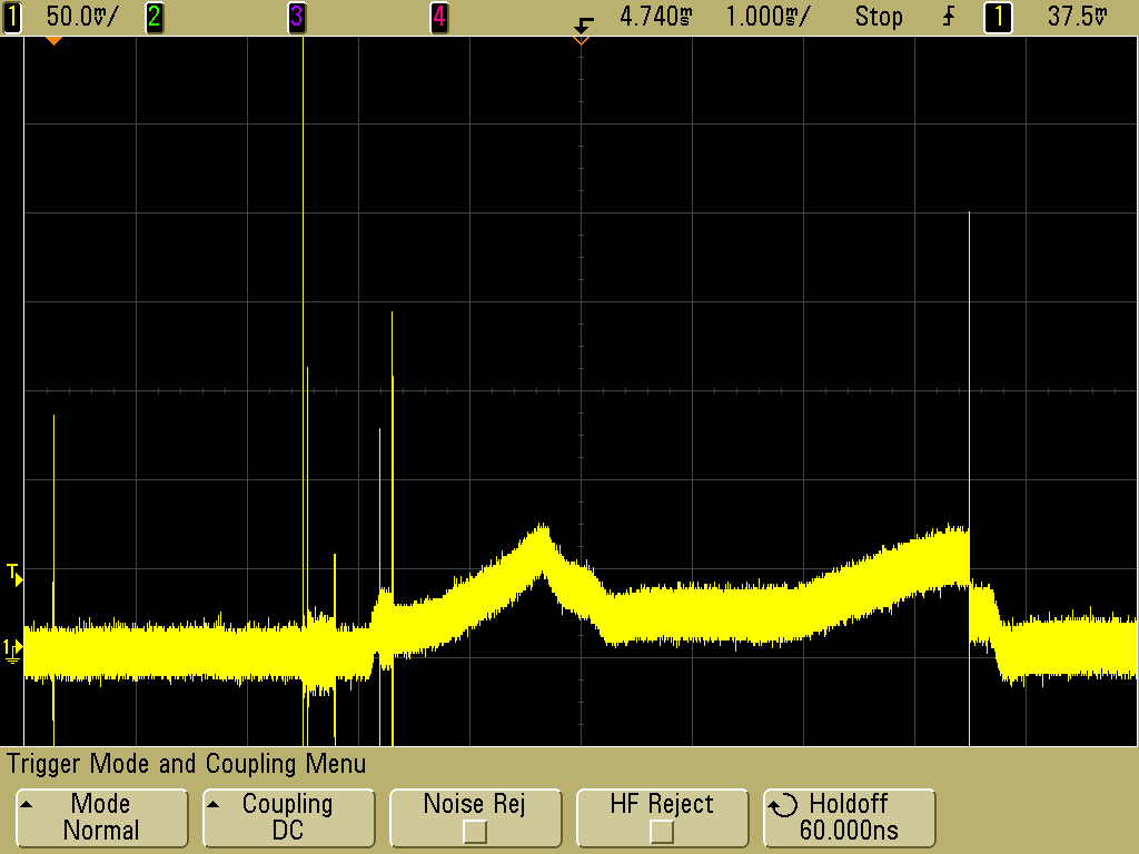
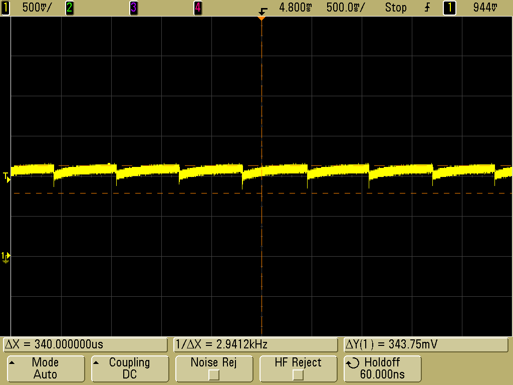
My TPS54318 circuit won't start; I get zero volts out.  I can see the SS pin ramp up to about 0.8V, and then drop to zero after about 3mS.  The enable is high.  Input voltage=5V.  

What's going on? I have no idea how to go about debugging this.

Thanks,

Barry

  • Hi Barry - could you share a schematic?

  • Attached (if I did it right) is the circuit .  Note there are 4 regulators.  The upper one (1V) works, the second one (1.8V) is the one I'm having trouble with (so far, as each regulator enables the one beneath it.)

    Note that only one of the four 261K resistors on the RT/CLK pins is installed.

    prosensing_PS.pdf
  • Attached is plot of startup signals.  Top trace is SS; bottom trace is EN.

  • For starters, I would recommend populating the RT resistor of each rail. The RT pin of these devices is very high impedance, so it will be noise sensitive if its not terminated locally. Also, I see there is a sync clock input on the schematic, what is this signal doing at this time? is it running, low, high-Z, etc?

    When you designed the loop compensation, was the additional capacitance (other than the 2x 10uF) applied?

  • Also, this is not normal behavior for SS. It should charge up to ~1.7V, well past the 0.8V Vref. 

    What do the Comp and RT pins look like?

  • Well, this is a chicken and egg kind of thing Ive gotten myself into.  The sync clock comes from an FPGA which is powered from this power supply.  Since the FPGA is not configured, the output driving REG_SYNC was somehow loading the RT input, and I observed the 1.0V output to have a very low frequency (about 50KHz) and about 500mV ripple.  I cut the trace and the 1V worked fine, so there's definitely some loading issue here (a problem for another day.  I believed the unconfigured FPGA output should have been HI-Z)).  So, REG_SYNC is not driven, but the four regulators have their RT inputs connected together.  

    I removed the other RT resistors because they are basically paralleling each other and would have presented too low a resistance.  I suppose I can use 4 1Meg resistors and get similar results.  But I don't think noise is my problem now.

  • COMP is sitting at about 1.7V; RT is about 0.5V

  • Hi Barry -Well, RT = 0.5V means that the device is "alive" internally. The 0.5V level is scaled from the internal LDO which supplies the logic of the device. 

    Comp = 1.7V also correlates. The Comp pin is the output of the error amplifier. Then VSNS cannot be pulled up to the 0.8V Vref, the comp voltage rises to command more duty cycle. Essentially it means the device is trying to pull the output voltage up (so the divided down version, VSNS can equal 0.8V), and cannot. 

    A few thoughts: 

    • Is there switching activity on the PH node?
    • Any chance the device is in current limit? 
      • You could add a wire loop in series with the inductor for a current probe. 
    • Also, if you unpower the board, and ohm across the output capacitors, is the output low-Z?
  • There is nothing on the PH output; it's stuck at zero volts (Blown output FET?) 

    The output measures about 4K-5K unpowered. I've disconnected the outputs from the rest of my board, so the only load should be the feedback resistors-about 27K.

  • Is there switching activity during the time when SS is rising? 

    Also, maybe double check the bottom feedback resistor? 

    If you think it might be blown power devices, you can ohm from VIN-PH (High-side FET), PH-GND, and the body diodes as for each FET as well. It's probably a good idea to lift the inductor when ohm-ing the FETs out. 

  • There's not really any switching.  I can see the output ramp up about 70mv (same rise time as the SS signal), it then drops back to zero after about 3mS.  see attached picture

    I measure about 3.6MEG  from PH to BOOT and about 3.6K from PH to ground (probably the resistor).  These values are similar to the working regulator.

  • Update: Bad TPS54318 was replaced, but still having problems.  1V regulator has a very ripple-y output, about 300mV peak to peak.  The period varies depending on the load (about 1 second at no load; about 330 microseconds at 1A load)  In neither case is the frequency anywhere near what's expected.

    Please help.  Is it possible to actually TALK to someone at TI?

    I've designed in four of these regulators on my board, and this is a BIG PROBLEM.  My design was based on values and components taken directly from WEB BENCH; the PCB layout is nearly identical to the recommend one in the data sheet.

    I've attached a scope capture of the 1 amp load condition.  I guess I can't attach two files.  I'll do that in the next post

  • Plot of no load condition

  • Hi Barry - Apologies. I am available for a call tomorrow, any time in the afternoon (EST). 

    Please e-mail me offline: mjschurmann [at] ti [dot] com to set something up. 

  • I looked at your schematic.  I think your problem lies in the lack of a pull up on your PWRGD signals.  I believe these are open drain and require a pull up voltage.  My next concern is the RT resistors.  For proper operation, each IC should have its own RT resistor located as close to the RT pin as possible and terminated directly to ground with as short path as possible.  If you are going to snyc multiple devices, I recommend individual buffered clocks to each device.

    Matt,

    Let me know if you need assistance with this or want me in on your call.

  • Hi John,

    According to the data sheet the EN pin (which is connected to the PWRGD of the previous regulator) has an internal pullup, so no external pullup is required.  It actually appears to be working that way on the board.  

    I now have the board configured so that each of the of RT inputs has a resistor right there. I'm using 1M, so that the parallel combination of the four resistors should make the effective RT=250k==> 750KHz switching frequency. I'm still seeing the same problem.

    Could the problem be that the four RT inputs are connected together? (Boy, I hope not)

  • I recommend not tying the RT pins together.  You could test this out to see if that is the problem.

    From the datasheet:

    "The PWRGD pin output is an open drain MOSFET"


    The EN pin does have an internal pull up, but it is pretty weak.  You have verified the the PWRGD to EN waveform is sufficient on your second regulator that is not coming up?  You could quickly try adding a 10k pull up to PWRGD.

  • I was actually going to suggest disconnecting the RT pins from each-other, just for an experiment. 

    John - We've set up a call today at 2pm EST. Message me offline if you're available to join so I can set up a meet-me number. 

  • Yes i have never seen these work well with the RT pins tied together.  That's 1 PM my time.  I'll check my calendar.

  • Ok.  I will cut the traces tying the four RTs together and change the resistors to 243K.

  • Ok!  So,  I cut the traces running to three of the four RT pins so that those regulators only have the RT resistors.  The fourth regulator was still connected to the trace, but the trace was cut so that there is nothing driving it.  The three disconnected regulators now seem to be very happy!

    However, the fourth regulator had a bunch of noise on it, both high-frequency switching noise (about 750KHz) along with about 15 KHz of 'other' noise.  I cut the trace running to the RT pin, and the 15 KHz noise went away, but I still have about 150 mV P-P of switching noise.  So,  apparently an unterminated trace of about 2" with several stub traces off of it was affecting the regulator.

    So now my problem is that 150mV noise on one regulator.See attached picture.

  • It seems the issue is that each device was trying to regulate its own RT pin to ~0.5V, and the different RT pins were "fighting" each-other. 

    As I mentioned earlier, the RT pin is very high impedance, so noise pickup on the RT pin is a real concern. 

    I assume we're looking at Vout here. Can I ask how well this was high-frequency probed (i.e. very tiny ground lead)? Could it just be pick-up from the scope lead? If it is real, we may need to look at the layout, or add some high-frequency output capacitors. 

    Also, does this HF noise show up at the load, or at the output of the regulator, or both... 

  • No, it was a crummy scope ground lead, but the same probe was used for looking at the other 3 regulators and I didn't see noise anywhere near that magnitude.  Yes I'm looking at Vout.  The layout for this problem child is identical to the other three, with different component values/output voltage/output current