This thread has been locked.

If you have a related question, please click the "Ask a related question" button in the top right corner. The newly created question will be automatically linked to this question.

LM27762: LM27762 startup issue

Part Number: LM27762
Other Parts Discussed in Thread: LM317, , TPS65132

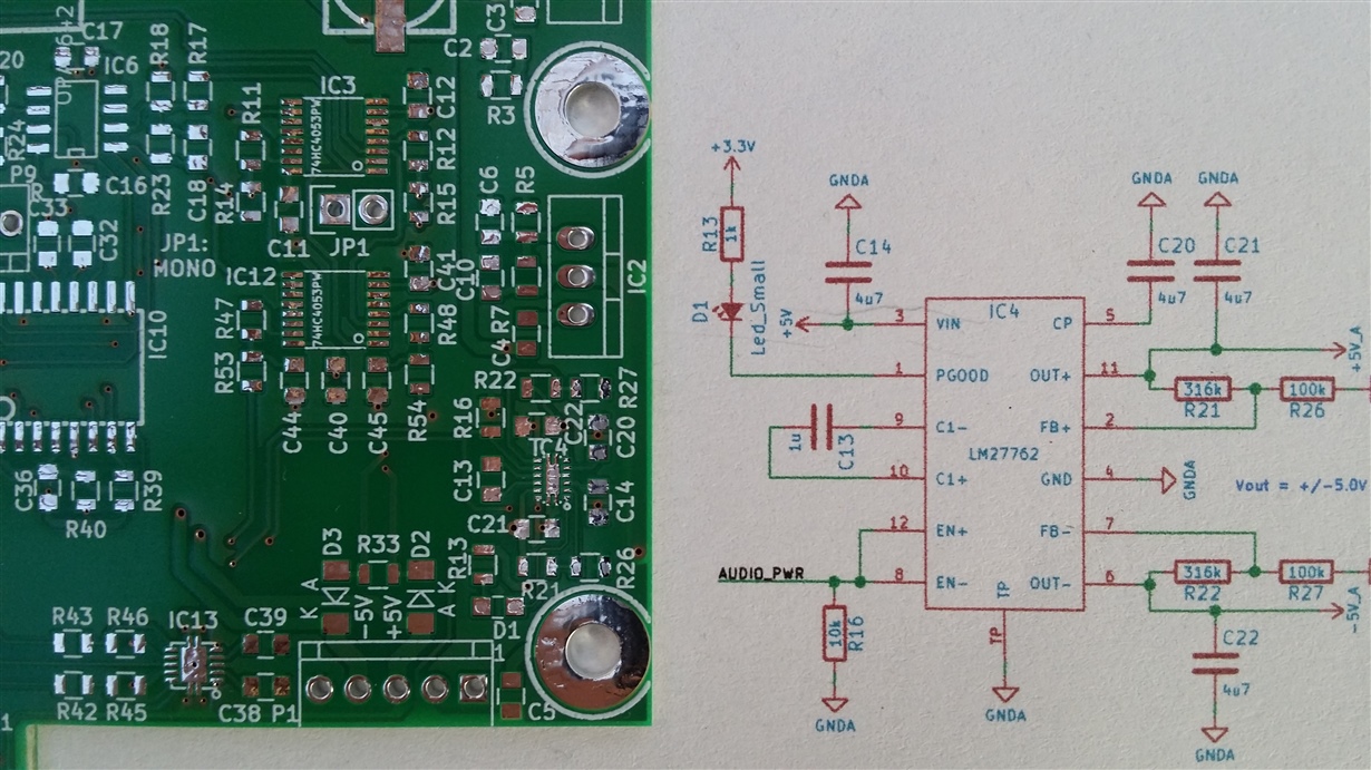
Hello, I'm having a little problem with the power supply for my audio design (see attached schematic). The idea of the power supply design is, to use a linear regulator (I use LM317T) to stabilize a DC input voltage to 5.3V. From the +5.3V I want to generate a +/-5V audio power supply for the analog circuit. The DC input voltag should be +8V up to +15V. The design works if the DC input voltag is about +7.7V ... +8.3V (stable +/-5V analog output voltage, LED is on) but if the DC input voltage is higher, the LED connected to PGOOD does not turn on and the negative output voltage does not go to -5V.  It looks as if the LM317 output cannot cope with the load represented by the LM27762. Any idea what goes wrong?

Andy

  • Andy,


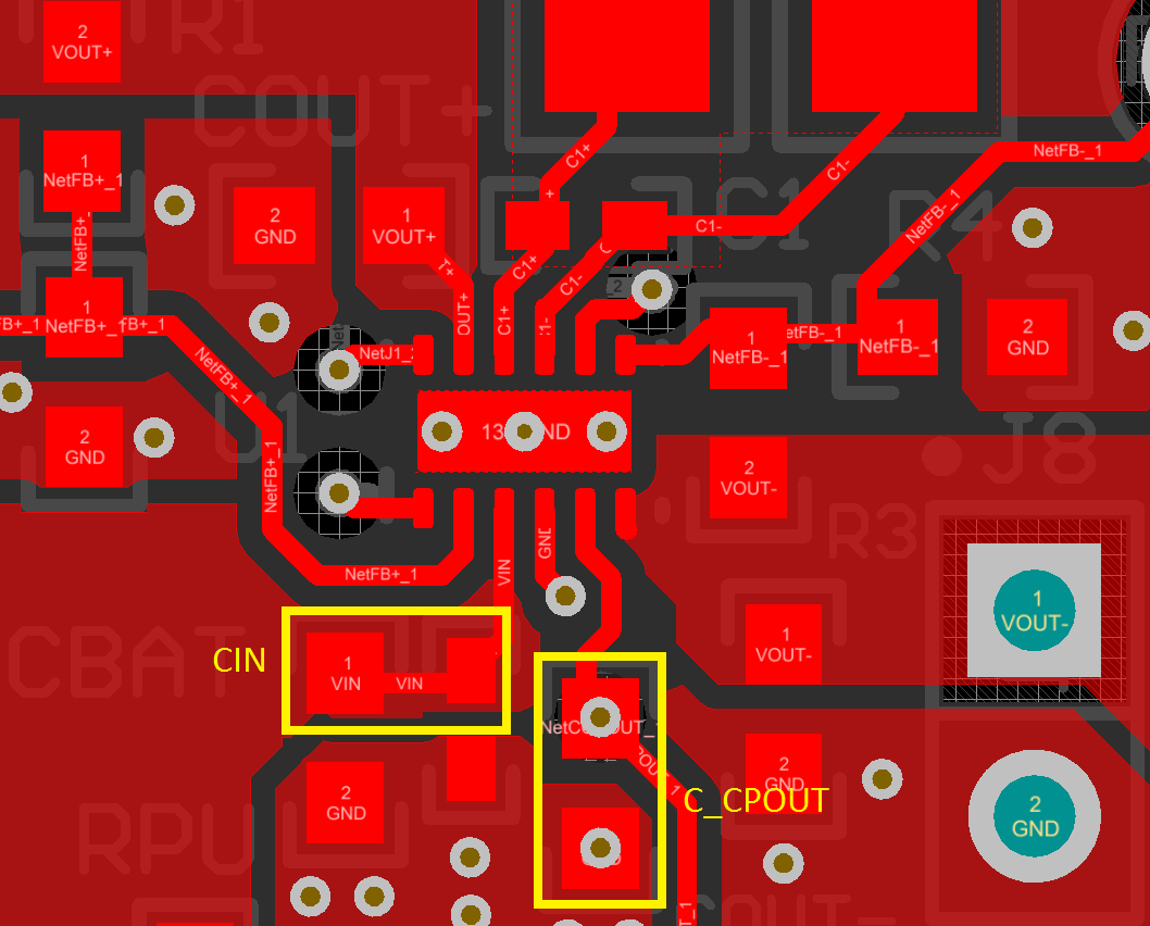
    Please provide layout figures of LM27762 and surrounding components. Typically start-up issues of negative output have been related to layout issues. (parasitic inductance in GND pin wiring).


     Regards,

    Juha

  • Hello Juha,

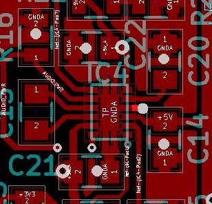
    super fast response, thank you. You might be right, the layout could be the problem. Attached are pictures of all PCB layers (it is just a 2 layer board) and a photo of the empty PCB. 

    Thank you for your support and best regards

    Andy

    Picture 1: Both layers

    Picture 2: Front layer

    Picture 3: Back layer

    Picture 4: Photo

  • Andy,

    Thanks for the layout figures. It looks like path from GND pin to ground plane could be shorter. This is from our EVM:

    Notice how GND pin is connected through via to GND plane. Similarly your board could be modified by adding via next to GND pin:

    Modification could be done to existing board if you have small enough drill bit.

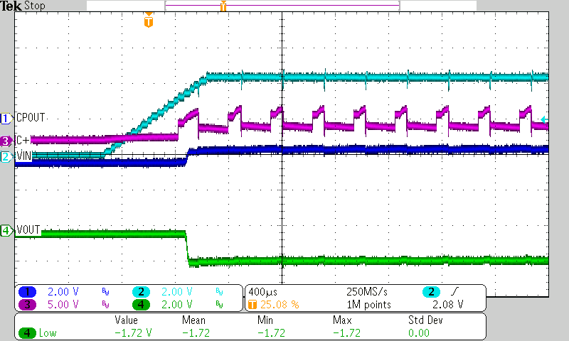
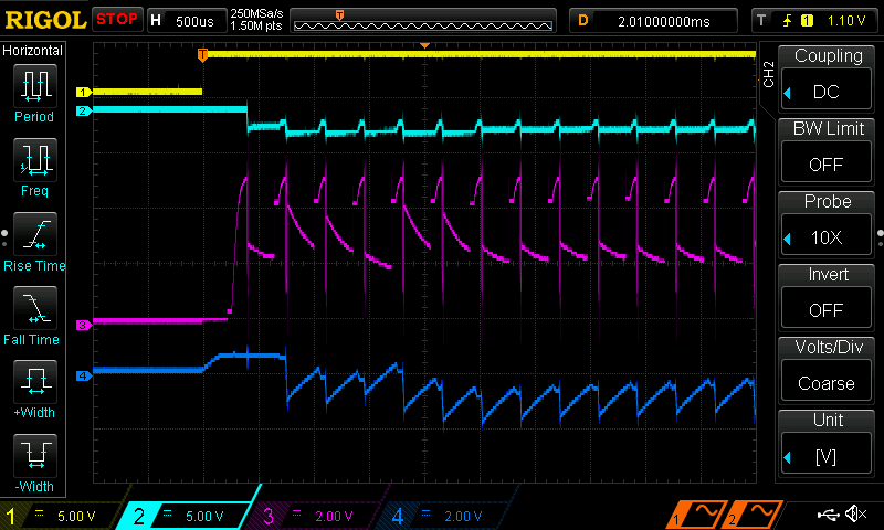
    This is the waveform in C1+ pin after failed start-up due to not so good layout:

    And this is the waveforms when charge pump is operating normally:

    Maybe you can compare these scope shots to your situation.

    Regards,

    Juha

  • Hello Juha,

    thank you for the hint. I did not manage to get it working yet but I keep trying.

    Best regards

    Andy

  • Andy,

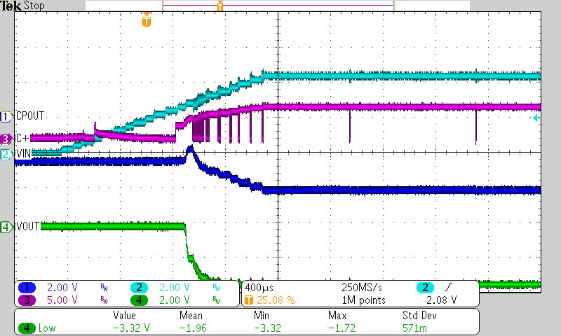
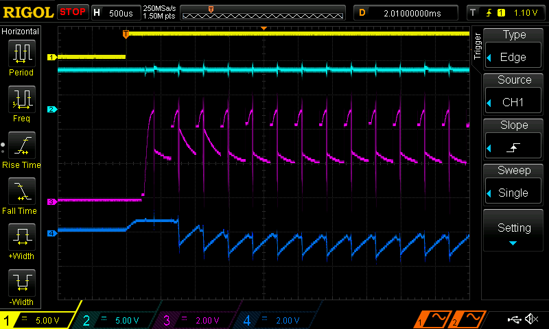
    If you can share oscilloscope shot of start-up (VIN,CPOUT,C1+,VOUT-,EN), I can take a look at it.

    Regards,
    Juha
  • Hello Juha,

    I have made some measurements. After power up, my CPU waits 100msec before EN goes high, therefore VIN (+5.3V) sould be stable at the moment the LM27762 gets enabled.

    Picture 1 shows: 

    CH1: EN

    CH2: VIN

    CH3: C1+

    CH4: VOUT-

    Picture 2 shows:

    CH1: EN

    CH2: CPOUT

    CH3: C1+

    CH4: VOUT-

    When measuring I sometimes manage to get the LM27762 working, in particular when it happens that I accidently short circuit the input voltage (VIN). In those cases the circuit seems to start up properly but unfortunately this is not repeatable and definetely not a solution for a production product.

    Thank you for any hints and best regards

    Andy

  • Hi Juha

    I connected the enable pins through a 1k ohm resistor to VIN an now the LM27762 starts up. It seems that controling the enable pins from the microcontroller causes the issue.

    Best regards

    Andy

  • Andy,

    Sorry for late reply, I was out of office last week.


    Looking at your scope shots, it seems similar to the malfunctioning case I sent picture of. I am little worried that you only masked the real issue by pulling enable pins up to VIN via resistors. I think it fixed the problem because device is now enabled earlier, VIN has not yet risen to its target voltage. Startup happens with smaller VIN => smaller in-rush currents. We have seen this exact behavior when debugging start-up issues caused by excessive parasitic inductance in GND path.


    Did you manage to modify the PCB layout in a way I suggested earlier?

    Regards,

    Juha

  • Hi Juha,
    I agree that my solution does not solve the root cause but at least it allows me to test and evaluate the Overall design.
    The PCB modification is not that easy to do so we need to assemble another prototype next week. I plan to modify the PCB before mounting the components - this should be easier to do. The WSON package does not make rework on the PCB easy. May I suggest to consider someting like MSOP package for this device?
    As an alternative to the LM27762 I consider using DC/DC buck converter for generating my +/-5V. Any suggestions for a low noise device?
    Regards
    Andy
  • Hi Andy,


    I understand - if the fix makes it possible to do further testing, it is good enough. About the PCB modification, my idea was to make additional via from GND pin to GND layer by drilling hole through the PCB and soldering wire in it. It is not very sophisticated method, but it should reduce the inductance of path to GND plane. I admit that it is challenging as the space for the drill hole is limited, but with very small diameter drill size it should be possible. If this would be done next to footprint, you really would not have to touch LM27762 itself.


    As for buck alternative, you can take a look at TPS65132. However it does not have negative side LDO if I remember correctly.

    Regards,

    Juha