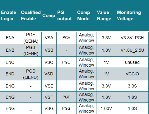
On page 138 of the data sheet and in the schematic in document number tidrco4.pdf the control for the VCCIO load switch comes from PGD, pin H3. The input for VSD, pin E6, comes from VCCIO which is the output voltage from the load switch. The VCCIO voltage must be good before it can turn on the load switch. How can the output of the load switch control the gate of the load switch and work?
-
Ask a related question
What is a related question?A related question is a question created from another question. When the related question is created, it will be automatically linked to the original question.


