A related question is a question created from another question. When the related question is created, it will be automatically linked to the original question.
If you have a related question, please click the "Ask a related question" button in the top right corner. The newly created question will be automatically linked to this question.
I see no evidence in the device datasheet of an output pulldown mechanism (ie load discharge). So, it is up to the load to pull output to 0-V. A resistive load should discharge the output cap to zero while a semiconductor type load may not. Try connecting a resistor from output to GND and see what happens.
If the semiconductor type load has other voltages (such as an IC with an IO and core voltage), leakage from the higher voltage source back to the 3.3V source can keep the output of the switch biased.
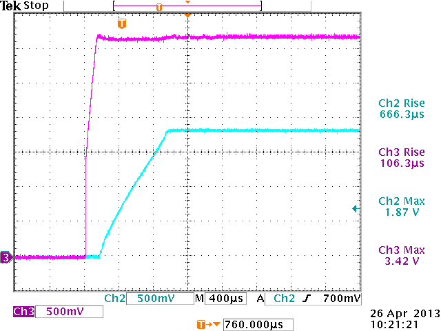
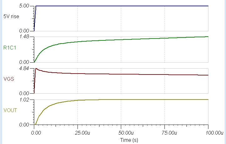
Here is a snapshot of the TPS27081 output (pink) where R1 = 10k, R2 = 0 and C1 = open. We have no 0.8V level between 0V and 3.3V. The total impedance seen by the switch is about 200 ohms when using this configuration.
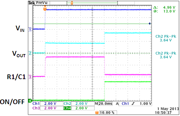
I tried adding a 200 ohms resistor at the output, because the load was about 20k (when R1 = 5.1k, R2 = 510R and C1 = 82nF) and its doing the same thing.
There is a FPGA and a HDMI receiver connected to this switch.
The TPS27081A is a P+N switch. Therefore it has all the disadvantages of a P+N switch.
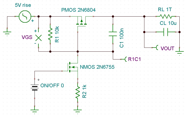
Before power is applied, the voltage on the "C1" capacitor (C147 is the first schematic) is zero. When power is applied to VIN (the PMOS source) the PMOS gate (R1C1) is zero volt and PMOS drain (VOUT) is also zero volts. Therefore the PMOS pass element is turned on by the low voltage on the R1C1 pin.
The 0V on the ON/OFF pin (NMOS gate) will keep the NMOS turned off. However the NMOS can not turn the PMOS off; it is only capable of turning the PMOS on.
I understand that, when VIN is rising-up, the voltage accros the capacitor C1 tends to stay at 0V for a moment (this the purpose of a capacitor). Since VOUT = 0V at T=0s, Vgate of the PMOS will tends to stay at 0V. So the PMOS will start to turn ON, because it's Vgs will be negative at this point. So you should expect a glitch at the output when VIN is rising-up.
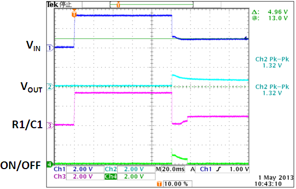
What I don't understand: after a moment, the voltage at the gate of the PMOS will change from 0V to about VIN.... so then, the PMOS should turn OFF again (unless the NMOS is turning ON...). What I measured is a Vgs of 0V on the PMOS, but the output is about 0.825V (VIN = 3.3V in our case and the ON/OFF signal is still 0V).... This 0.825V voltage shouldn't come from another power supply, since only removing R2 correct this problem!!!?!
Can you explain me what is wrong with my conclusion? (since my theory and the practice are not in sync!)
There is a lot of data in this forum thread and my earlier explanation may not cover everything that is happening. I will need to do some simulation and or take lab data to explain all the waveforms posted.
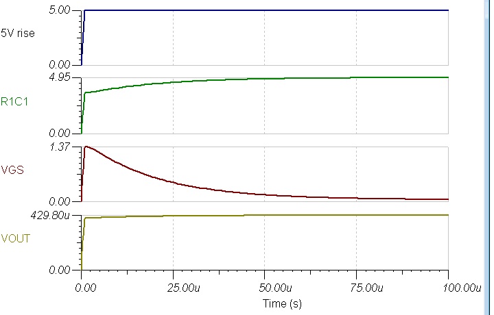
The uncharged capacitor from R1C1 to output will turn the output on when VIN is applied. This is the schematic I simulated. The MOSFETs in schematic have higher VT than the TPS27081 so I increased VIN to 5V.
This is the resulting waveforms. The output partially powers up as I predicted in an earlier post.
I also attached the TI-Tina (free simulator) file.
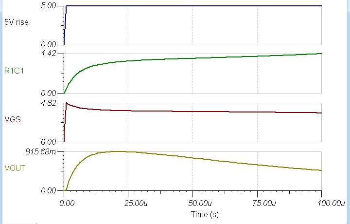
These waveform look like something is broken. The ON/OFF pin looks like it is "shorted" to ground. The output looks overloaded and is using more current than the main power source can supply so VIN drops.
Is the TPS27082L package could be an alternative to our problem? I see in the datasheet it has an excellent OFF isolation under transient. Thanks, Jérôme
I am looking into the TPS27082 design to see if that will be a good solution.
I checked the design and the TPS27082L will have much improved performance over TPS27081 for VIN rise-time immunity. The TPS27082L will short out R1 with ON/OFF pin is low.
R2 pin will be a ground pin on the "082L" device and the R2 function will be an internal fixed 12.5k resistor.
The TPS27081A is just a NMOS+PMOS switch. Nothing more, nothing less.
The TPL27082L has more circuitry. The data sheet front page says "TPS27082L features a novel OFF isolation circuit that prevents PMOS from turning ON in applications that may have fast transients, at the VIN pin when the load switch is in the OFF-state."
1. removing C1 reduces both rise and fall time for both devices.
2. rise time of 82L with internal 12.5Kohm R2 is smaller than 81A with external 3.16Kohm R2.
3. 82L’s improvement on falling time is very obvious!
Deep thanks for measuring the real waveform for us, I appreciate the work.
I would like to ask two additional questions:
1. Since both devices are rated as 3A current grade, would the results change significantly if we use a smaller RL, say 2ohm or 1ohm? Could the measurement be done again, only for TPS27082L, and without C1?
2. Can the device (TPS27082L) sustain repeated 1A-3A pulse 200μs at 200Hz? Would such periodic strong pulse change the performance measurement as comparing with individual, low current squares?
Hi Denis!
I have the same thought as yours. I think after a while, the output should decrease to zero rather than stay at 0.8V. That's very strange.
do you have any progress in this question?


