This thread has been locked.

If you have a related question, please click the "Ask a related question" button in the top right corner. The newly created question will be automatically linked to this question.

LMR14050-Q1: LMR14050-Q1's Temp and Switching ringing Issue (EMI)

Part Number: LMR14050-Q1

Hi. 

I using LMR14050-Q1(Spread Specrum Version) and I have two issues.

Please help me and let me know.

1) LMR14050-Q1 is more hot than another DCDC. How can I lower temperature?

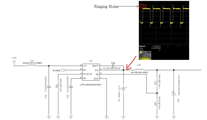
2) EMI Issue. According attached SCH and switching Pulse, switching pulse has ringing noise. How can I remove this ringing noise?

And what point is EMI debugging point?

Please help us.

Thanks.

  • Moving to the Simple Switcher forum...

  • Thanks for moving this topic John.

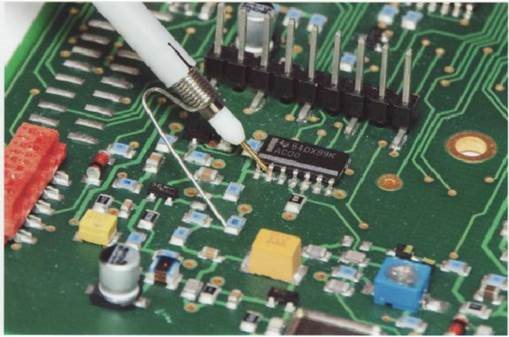
    The ring on the switch pin appears to be due to the probe method. You cannot use the clip-on ground lead of a scope probe. It needs to be either a probe tip receptacle (rarely done) or a pice of bare wire soldered to ground and wrapped around the metal ground barrel of a dismantled probe tip.

    The EMI test point location? There are three.

    1) The output terminal of L13 that leads over to IC pin 1 is where you begin the study for differential conducted EMI. Using a spectrum analyzer (with dc block!) you can determine how many dB attenuation is needed by the input filter comprised of L13 and a necessary input cap that needs to be added to this schematic.

    2) The true EMI test point would be made some distance away using a LISN and source wiring appropriate to the CISPR standard in effect. CISPR19,22,and 25 being most common.

    3) The residual output noise that leaves Cout is generally not referred to as EMI, but is important for the system so far as the load of this supply is concerned. Measuring at the load is the most important but begin by measuring just past Cout.

    Recognize that the switcher inductor and Cout form a two pole low pass to filter to the switching frequency. However, there are a number of parasitic terms not revealed by the schematic. In particular, the shunt capacitance of the inductor and the mounting inductance of Cout place a high pass filter directly in parallel with the low pass which is why there are always spikes on Vout corresponding to the switch transition. This HF spike stays at the same frequency even when spread spectrum is employed BTW. It is only the sidebands of the spike that will change with switch frequency.


    The output resistors in your schematic will result in 12V output. But the input voltage is labeled 12V. The switch waveform Is a fairly wide duty factor so roughly 16V input; can you confirm? The heat factor when running at such high duty cycles where Vin is fairly close to Vout will be more noticeable. How much current is the stage being asked for? 12Vout * 5A = 60W. 90% efficiency would be wishful thinking and cause 6W wasted power, most of it in the IC.

    Alan Martin
  • Hi,

    1) How large is your load? The power loss is larger as long as the output power is larger. Assume the output power is as high as 9V/4A, then lower frequency is preffered, 400kHz for example. Also large GND area surrounding the IC thermal PAD is preffered for better heat dissipation.

    2)Just as Alan mentioned, make sure you measured the SW waveform correctly. Usually we measure it with a short probe to avoid noise interruption. Just like below picture. A boot resistor in series with Cboot, or an RC snubber parrel with the schottky diode will damp the ringing, however it may lower the efficiency, and result in more power loss and heat.

    EMI generates at where large dv/dt or di/dt happens. That's where you need to pay attention to. For DC/DC, it's the discontinuous input current which has large di/dt and the SW node which has large dv/dt.