This thread has been locked.

If you have a related question, please click the "Ask a related question" button in the top right corner. The newly created question will be automatically linked to this question.

CC256x Power Control Step Specification

Other Parts Discussed in Thread: CC2564

Hi All,

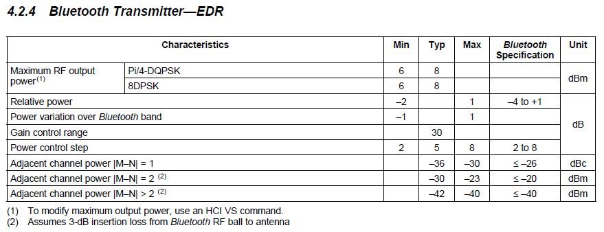
Is there a clear method as to how the Power Control Step is characterized per the CC2564 datasheet?

As indicated in the 4.2.4 Bluetooth TX - EDR datasheet section, if the device uses the Typ 8dBm output power (MAX specification is not provided), what variation (MIN to MAX) should be expected at the Antenna?  I see Note 2. Assumes 3-dB insertion loss from Bluetooth RF ball to Antenna.

However, the CC256x VS HCI Commands Wiki indicates that the default MAX TX power defined in the SP is +12dBm and corresponds to Power Level 15.  If this accurate for the MAX TX value, then I would expect the MAX power control step specification to be as high as 9dB and above the Bluetooth Specification range.

Am I missing something here?

Thanks,

Robb


  • Hi Robb,

    I will check internally and get back to you.

    Regards,
    Gigi Joseph.
  • Hi,

    The typical value is 8dBm. The min max would be 6,10 dBm.
    Max Tx power of 12dBm which is set by the VS command is at the antenna ball. If you have a filter of 3dB, you would see 9dBm.

    Regards,
    Gigi Joseph.
  • Hi,

    I guess the question is more connected to the Power Control Step.  

    Does the CC2564 implement any optimization for TX power levels automatically in hardware?  Are there any other TX output level used other than the 8 indicated on the TI Wiki (+12, +7, +2, -3, -8, -13, -18, -23dBm)?

    Thanks,

    Robb

  • Hi everyone,
    This is Sang working for Intel and I originally asked this issue to Robb.

    Yes, Robb is right.
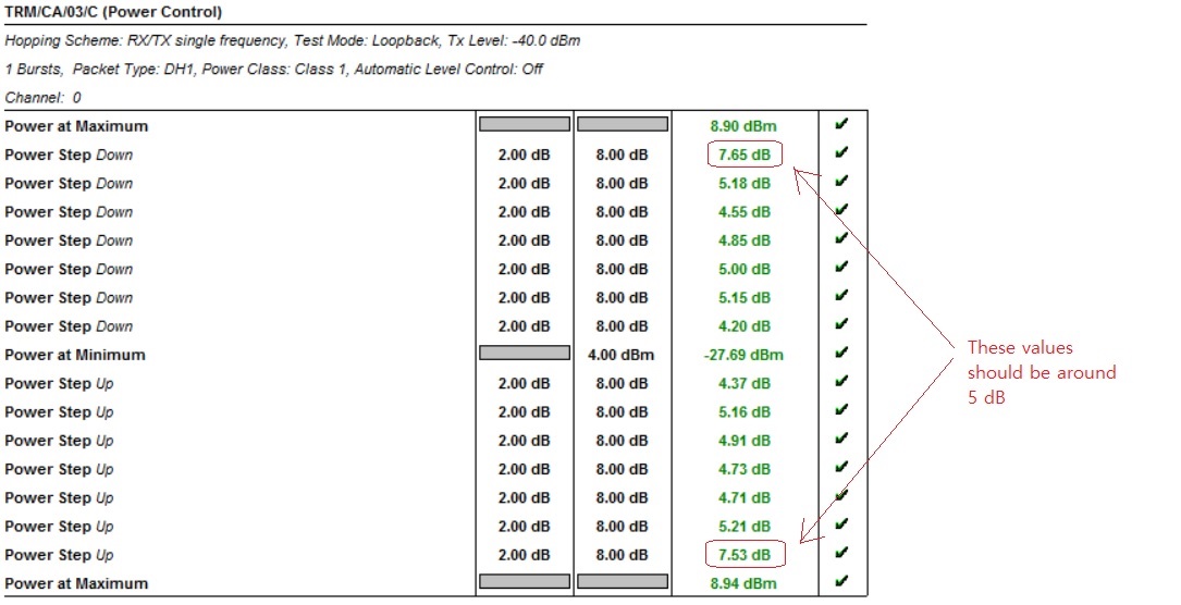
    The power control step should be 5 based on the Typ value but currenlty my board has different results per channels.
    One step down command from equipment should make +12dBm to around +7dBm but my board goes down to +3.8dBm for some channels and the limit is +4dBm for this example.(These are not absolute value of my board, I just changed the values for easy understanding.)
    I have tested two different version of PCB and both have the same result.

    Do you have anything to change the step size or to fix this issue?

    Thanks,
    Sang
  • Sang,

    The power levels can be changed using the following command: http://processors.wiki.ti.com/index.php/CC256x_VS_HCI_Commands#HCI_VS_DRPb_Set_Power_Vector_.280xFD82.29 

    Note that it is recommended to change the Max Output Power only using the BHET tool and leave the 5dB step/level.

    Regards,

    Miguel

  • Hi Miguel,

    Thank you for letting me know the command.
    I have reviewed it and found there is no section to set frequency for the Max Output Power.
    Below is the result for my board.

    TRM/CA/03/C (Power Control)
    Packet Length Tested: DH1
    Hopping OFF Low Med High Limits
    Max Power 8.60 dB 9.40 dB 6.80 dB
    Min Power -4.60 dB -1.90 dB -1.20 dB
    Max Power Step 8.10 dB 6.40 dB 8.10 dB <= 8.00 dB
    Min Power Step 5.30 dB 5.00 dB 8.10 dB >= 2.00 dB
    Total Packets Failed 2 0 2
    Total Packets Tested 4 4 2
    Result Fail Pass Fail

    As you can see, Max and Min Power Step results are different through the frequenies and I believe those values should be around 5.
    I am not sure if I can fix it by changing Max Output Power.
    Can you please double check with above result and let me know your opinion?.

    Thanks,
    Sang
  • This is the result with good format.

    TRM/CA/03/C (Power Control)
    Packet Length Tested: DH1
    Hopping OFF Low Med High Limits
    Max Power 8.60 dB 9.40 dB 6.80 dB
    Min Power -4.60 dB -1.90 dB -1.20 dB
    Max Power Step 8.10 dB 6.40 dB 8.10 dB <= 8.00 dB
    Min Power Step 5.30 dB 5.00 dB 8.10 dB >= 2.00 dB
    Total Packets Failed 2 0 2
    Total Packets Tested 4 4 2
    Result Fail Pass Fail

    Thanks,

    Sang

  • Sang,

    Which device are you using?Is it your own QFN on-board? At which point are you measuring this? Which Service Pack did you use? How did download it?

    ~Miguel

  • I am using CC2564B, BT4.0 + BLE, supporting HFP and A2DP and it is placed on my own board.
    Schematic is configured to Full DC2DC power scheme and it means 1.8V is supplied to CL1.5_LDO_IN, MLDO_IN and MLDO_OUT pins.
    Saw filter and Diplexer are placed between CC2564 and Antenna.
    Regarding Service Pack, I will update it once I get it from SW team.

    Thanks,
    Sang
  • Sang,

    Ok. Let me know which SP you are using. Regarding the measurements, at which point on the RF trace are you measuring it?

    ~Miguel

  • Hi Miguel,

    I have measured it at between Diplexer and Antenna.
    It means Diplexer and BPF are included in the RF path.

    The Service Pack downloaded in the BT TI Chip comes from processors.wiki.ti.com/.../CC256x_Downloads web page.
    We use the “CC2564B BT 4.0 SP” file.

    Thanks,
    Sang
  • Sang,

    Could you measure it before the diplexer? i.e. right after the BPF

    ~Miguel

  • Hi Miguel,

    I have measured it before the diplexer and got same result for the power control steps.
    Max output power is somewhat flattened since the trace is not passing the diplexer.
    It looks like related to RF power sweep calibration.
    Can you please check if the parameters for the RF are different for each of the power schemes.

    Thanks,
    Sang
  • Sang,

    Which BT tester are you using? Also, were you able to confirm the SP version? And any modifications to it that might have been applied?

    Regards,

    Miguel

  • Hi Miguel,

    I am using Anritsu MT8852B BT/BLE Tester.
    Regarding SP version, I am going to ask to SW team and will let you know.
    What kind of modification are you asking?. About RF side modification on SW?

    The problem looks like RF output power versus power levels are not calibrated correctly or missing.

    Thanks,
    Sang
  • Sang,

    Yes, it looks like a wrong calibration. The reasons why it would happen this scenario is if the Service Pack is incorrect, the SP is modified incorrectly and/or the Power Vectors are modified incorrectly. This would happened during device initialization.

    Regards,

    Miguel

  • Hi Miguel,

    As I heard from our SW team that they did not apply any modification on RF side.

    I have attached the header file from them.

    Thanks,

    Sang

    bluetooth_init_cc2564B_1.0_BT_Spec_4.0.h

  • Hi Sang,

    The array is not correct. It should start with a 0x01. Also, the rest of the bytes do not reflect a proper format. How did you get these array?

    ####################### Your Array - Incorrect ##########################

    /*
     * PatchRam for Bluetooth Texas Instrument CC2564B Chip */
    const char BasePatch[] =
    {
    0x42, 0x54, 0x53, 0x42, 0x01, 0x00, 0x00, 0x00, 0x00, 0x00,
    0x00, 0x00, 0x00, 0x00, 0x00, 0x00, 0x00, 0x00, 0x00, 0x00,
    0x00, 0x00, 0x00, 0x00, 0x00, 0x00, 0x00, 0x00, 0x00, 0x00,
    0x00, 0x00, 0x06, 0x00, 0x52, 0x00, 0x23, 0x2d, 0x2d, 0x2d,
    0x2d, 0x2d, 0x2d, 0x2d, 0x2d, 0x2d, 0x2d, 0x2d, 0x2d, 0x2d,
    0x2d, 0x2d, 0x2d, 0x2d, 0x2d, 0x2d, 0x2d, 0x2d, 0x2d, 0x2d,
    0x2d, 0x2d, 0x2d, 0x2d, 0x2d, 0x2d, .....

    ####################### Correct SP array ##########################

    static BTPSCONST BTPSVEND_PATCH_LOCATION unsigned char BasePatch[] =
    {

       0x01, 0x37, 0xfe, 0x02, 0x07, 0x10, 0x01, 0x05, 0xff, 0xff, 0xd0, 0x62, 0x08, 0x00, 0xfa, 0x07,
       0x10, 0x47, 0x0d, 0x00, 0x00, 0x00, 0x00, 0x00, 0x00, 0x00, 0x00, 0xf0, 0xb5, 0x88, 0xb0, 0x02,
       0x90, 0x47, 0x68, 0xff, 0x20, 0x26, 0x30, 0xc0, 0x5d, 0x00, 0x28, 0x26, 0xd0, 0x01, 0x38, 0x1d,
       0xd0, 0x01, 0x38, 0x2a, 0xd1, 0xff, 0x24, 0x95, 0x34, 0xe5, 0x19, 0x29, 0x88, 0x08, 0x20, 0x01,
       0x26, 0xb6, 0x46, 0x39, 0x4a, 0xfe, 0x44, 0x10, 0x47, 0x00, 0x29, 0x01, 0xd1, 0x02, 0x20, 0x07,
       0xe0, 0xe5, 0x19, 0x29, 0x88, 0x08, 0x20, 0xb6, 0x46, 0x34, 0x4a, 0xfe, 0x44, 0x10, 0x47, 0x48,
       0x1c, 0xe9, 0x88, 0x0c, 0x1c, 0x44, 0x43, ....

    ~Miguel

  • Hi Miguel,

    I am working on this project with Sang,
    Regarding the patch version, we were using an old one 6.6.15.
    We have updated the patch version 6.7.16, which is the latest one from the TI website.
    With this version the problem is still present.
    (FYI, regarding the patch version above, there is one additional header added by a third-party SW, that is removed during the download. This is why you did not recognize it the patch.

    On our product, we have now the capability to send HCI VSC raw commands so that we can any commands
    From the below page:
    processors.wiki.ti.com/.../CC256x_VS_HCI_Commands
    there is a VSC command for Calibration + VSC commands to read/write internal registers.

    From those commands, may be you can suggest us a sequence of commands that we can execute,
    and report back the results to you to help us supporting this issue.

    Br,
    Franck
  • Hi Miguel,

    I am a SW guy working on this project.
    We were using an old patch and by using the latest version 6.7.16 from TI website,
    the problem is still present.
    FYI, in your previous update, you did not recognize the patch because there is a
    header added by a third-party SW, that is removed when downloading the patch into
    the TI chipset.

    On our board, we have the capability to send HCI VSC raw commands.
    From the link below :
    processors.wiki.ti.com/.../CC256x_VS_HCI_Commands
    There are some commands for calibration and read/write internal registers.
    From those commands, could you recommend us a sequence to execute and then
    we report back to you the results, to help you supporting us on this issue.

    Br,
    Franck
  • Hi Franck,

    I recommend using the BHET tool to change the output power rather than sending the raw HCI VS commands. Note that there are specific command sequences and parameter considerations that have to be taken into consideration which it is easier to make a mistake.

    Regards,

    Miguel

  • Hi Robb,

    I think the MAX TX power +12dBm is measured at the ball of chip.

    I see average 9dBm Max output power in my device with about 2.5dB IL from ball to Antenna.

    Thanks,

    Sang

  • Hi Miguel and Robb,

    As you can see in below result, Only the step from or to Max power has a big value and it means I am using wrong calibration table since all the units I have showing similar result with below.

    Can you please let us know which file or data we have to use and how to check if the cal table on our device is correct.

    Please give us very clear and detailed description not to ping pong so long since this issue is pretty obvious and you know the solution.

    Thanks,

    Sang

  • Hi All,

    Thank you so much for all you guys to help me to solve this issue so far.
    Fine tune for the Tx matching values solved this issue.
    It was not a calibration issue.
    I am not sure why only the maximum output power is affected by the matching values but it is true.
    I have thought that the power control step is relatively managed by TI chip but the truth is that the values for each Tx steps seems like absolute ones.

    Anyway, it is fixed.

    Thanks,
    Sang
  • Matching change fixed this issue.