

Innovation in packaging matters, especially when it comes to designing a MOSFET nearly the size of a flake of pepper – the perfect size to fit into next generation portable designs that support higher currents than ever before.
Designers of computing, industrial and telecom power applications typically use discrete MOSFETs to achieve power efficiency with higher current rails -- but the trick is to design the smallest form factor as possible. Now designers can combine high-efficiency, low on-resistance and the industry’s smallest size with TI’s new Power Block II family of synchronous buck NexFET™ power MOSFET pairs.
The new ultra-thin Power Block II devices allow products to become dense, while consuming less power and dissipating less heat.
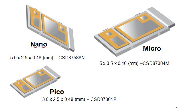
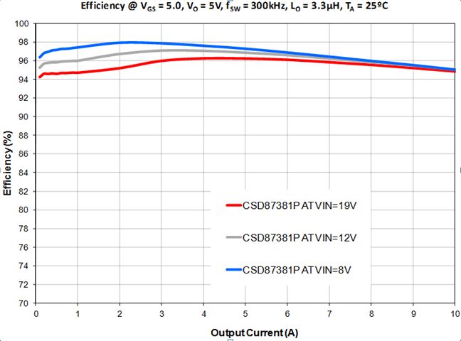
With a body size as small as 2.5 mm by 3 mm, and a height of less than 0.5 mm, the incredibly small devices enable thin and light designs with the lowest possible on-resistance. Power Block II improves efficiency over standard discrete MOSFETs, resulting in significant power savings.
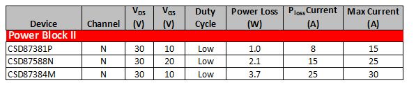
Power Block II uses an innovative clip style LGA package to mount 2 discrete MOSFETs in a half bridge configuration. This allows maximum silicon content for lower on-resistance and small size. The device family can generate 15 A to 30 A of continuous current. They also have DualCoolTM capability, allowing topside cooling with a heat sink to support higher currents. In addition to better thermal performance, the new Power Block II packaging is ROHS compliant and completely halogen- and lead-free.
Additional Resources:
