

This technical article was updated on July 23, 2020.
As with any complex analog circuit, designing SAR ADC circuits involves multiple tradeoffs and is thus an iterative process. Thanks to SPICE simulation tools, such as TINA-TI and TI's Precision SAR ADC models, accurate computer-based performance estimation after each design iteration is relatively quick and painless.
The most important tradeoffs in SAR ADC applications involve accuracy, response time and power consumption. These parameters are inter-dependent, and must be traded off per application requirements. Indeed, the greatest value of a SAR ADC is in its power-scalability with sampling rate. Due to this property the power consumption of the ADC input drive circuits may dominate at the system level, and using low power components becomes necessary. The problem is that low-power drive circuits generally have higher output impedance, which translates to slower response and lower accuracy. Thus, careful design choices are required to achieve an optimal trade-off, and therefore the primary focus of our SAR ADC models is to accurately represent factors that modulate ADC accuracy and power consumption, so that users can optimize the ADC input drive circuits accordingly.
Figure 1 depicts the TINA-TI models of two popular high-precision SAR ADCs – the ADS8860 and the ADS8353. Both are 16-bit 1MSPS devices, but unlike the ADS8860, the ADS8353 contains two 1MSPS simultaneous-sampling ADCs. Both ADC models have several commonalities that make them functionally equivalent to each other.
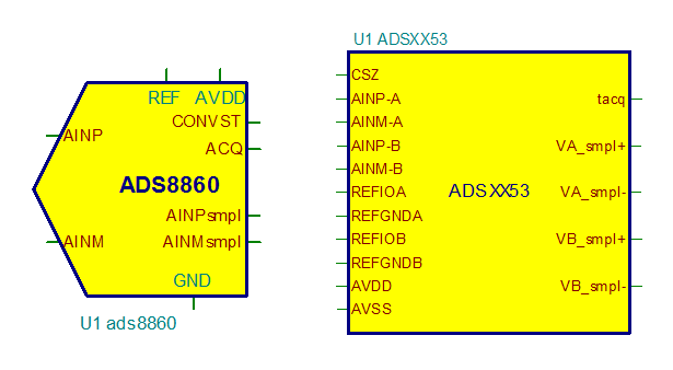
The inputs to each TINA model include the power supply, input, reference and “CONVST” or “CS” signals, which are defined in the datasheet. The outputs of each TINA model are “tacq” or “ACQ”, which indicate whether the ADC is in acquisition or conversion mode, and the “*smpl” signals represents the acquired input voltage values.
To see how well a SAR ADC TINA model correlates with the device datasheet, we can run a quick set of simulations using ideal input sources to drive the ADC model. For convenience, we use the ADS8860 TINA model as shown in Figure 2.
First we find the DC operating conditions of the circuit:

Figure 2: TINA schematic and simulation of DC operating conditions
When the ADC is not converting, it enters a “power-down” state, drawing about 50nA of current from AVDD. With ACQ high (3V logic), the ADC is in acquisition mode. Naturally, the sampled signal (AINPsmpl – AINMsmpl) is the same as the DC input (AINP – AINM) at 2.5V, and the supply current is about 30nA, indicating “power-down” mode operation.
Next, we simulate the ADC’s dynamic behavior through a transient analysis of the circuit for a full-scale 40 kHz sinusoidal input. The average values of the supply and reference currents can be precisely determined by extracting the DC components of their Fourier Series expansions as shown in Figure 3.
(Click on image to enlarge.)
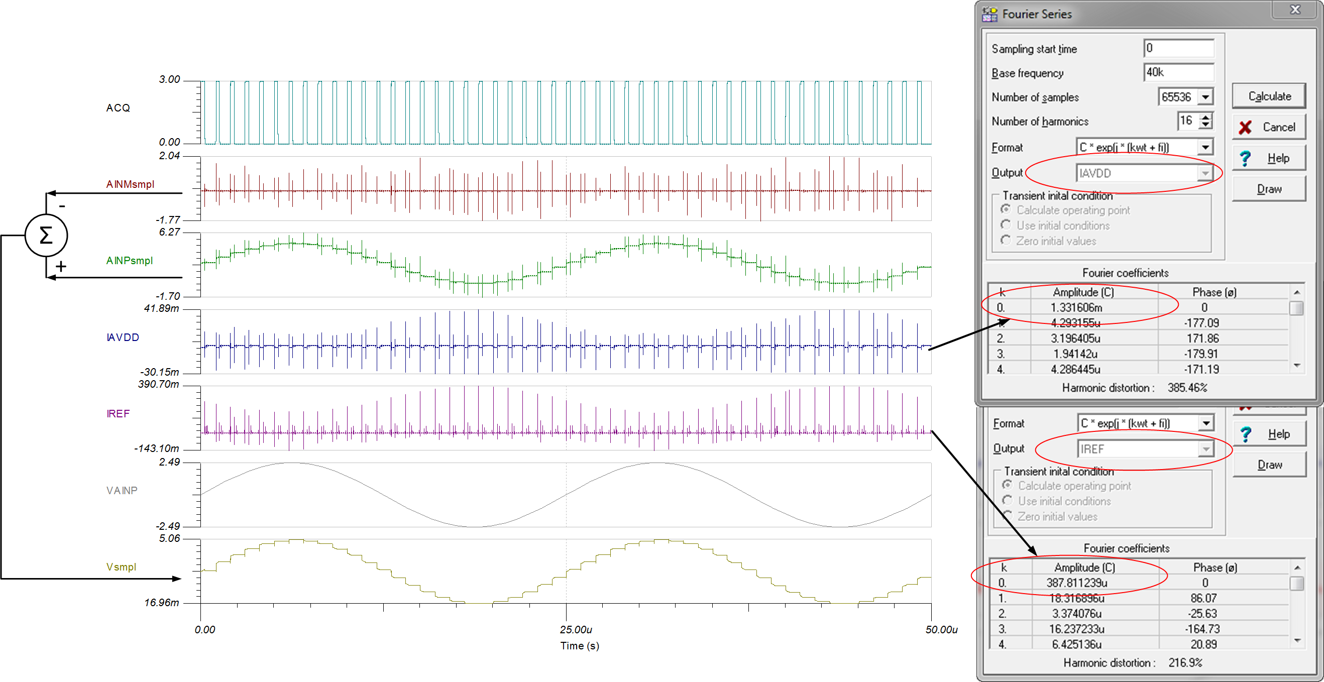
Figure 3: Transient analysis of ADS8860 showing RMS values of supply and REF input currents
Once again we observe that the TINA model provides good approximations of the supply and reference input currents. Typical datasheet values are 1.8 mA and 300 uA respectively at 1 MSPS. Additionally, “Vsmpl” in Figure 3 clearly illustrates the sample-and-hold behavior that is fundamental to the SAR ADC architecture.
The technique illustrated in Figure 3 can be used to verify ADC power-scalability vs. sampling rate. Figure 4 depicts average IAVDD vs. sampling rate obtained by sweeping the CONVST frequency.
(Click on images to enlarge.)

Figure 4: Comparison of TINA model estimate vs. datasheet plot of supply current vs. throughput
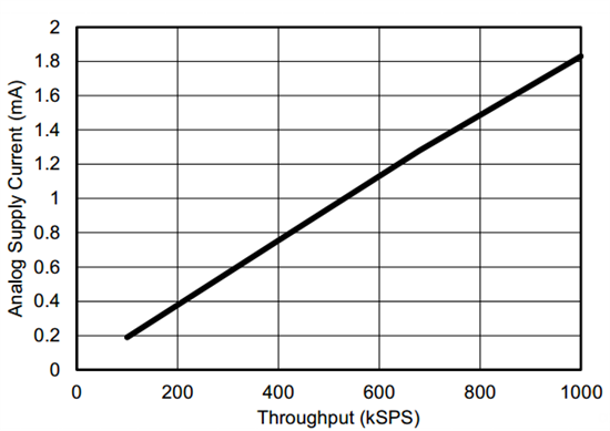
Figure 4: Comparison of TINA model estimate vs. datasheet plot of supply current vs. throughput
The simulation results differ from the datasheet in terms of the absolute current values at each sampling frequency, and this is probably because the TINA model may be based on IC simulation data vs. actual device test data that the datasheet uses. However, the simulation results do confirm the strong linear relationship between ADC supply current and sampling rate.
In conclusion, the TINA model emulates a real SAR ADC in terms of static behavior and power scalability versus throughput.
Stay tuned for a follow-up blog post in which we examine how a SAR ADC model can be used to understand the effect of source impedance on ADC accuracy.
Related resources:
Read more about SAR ADCs on the Precision Hub.
See an overview of TINA TI.
ADS8860 tools and software
ADS8353 tools and software
