

This post is co-authored by Richard Barthel and Errol Leon.
In applications such as position sensors, data-acquisition systems and resistance temperature detectors (RTDs), it is important to design with high precision in mind. In many cases, designing with precision integrated circuits (ICs) reduces signal-chain complexity, lowers the external component count, and minimizes board space and bill of materials (BOM) costs. The inaccuracies of one device may propagate through with the inaccuracies of another device, resulting in undesirable and unpredictable errors. In the case of a buffer-configured operational amplifier (op amp) at the output of a digital-to-analog converter (DAC), it’s crucial that your DAC and your op amp are precision devices for an accurate output.
A traditional rail-to-rail complementary metal-oxide semiconductor (CMOS) amplifier architecture includes two differential pairs, PMOS (blue) and NMOS (red), shown in Figure 1. Together, these two transistor pairs span the entire input common-mode voltage range. When one transistor pair takes over from the other, however, a unique and nonlinear phenomenon known as “input crossover distortion” occurs due to the intrinsic input offset voltage of each of the two input differential pairs, shown in Figure 2.

Figure 1: Traditional rail-to-rail CMOS amplifier architecture

Figure 2: Input offset voltage vs. common-mode voltage
When you connect a traditional rail-to-rail CMOS op amp at the output of a high-precision DAC, the crossover distortion will introduce an error and result in a drastic increase in integral nonlinearity (INL). This may cause the signal to deviate several least significant bits (LSBs) from its ideal value.
Now, what does 1LSB mean? Equation 1 is a simple equation to calculate LSB:
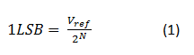
where N is the DAC’s number of bits.
The DAC8830 is a 16-bit DAC. If the voltage reference is Vref = 5V, then:
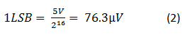
So to deviate more than 1LSB means that you can have more than 76.3µV of error at your output. This can be detrimental to many precision applications, like critical systems where failure has the potential to negatively impact customers’ end products.
So how do you fix this? Enter zero crossover!
You can span the entire input common-mode voltage range by using a zero-crossover op amp such as the OPA388. The zero-crossover topology uses an internal regulated voltage charge pump to increase the positive supply voltage and thus achieve linear operation with input common-mode voltages all the way to its rails with a single input transistor pair, shown in Figure 3. This results in true rail-to-rail input operation without a crossover region, and thus no crossover distortion. If you were to connect this kind of op amp at the output of a DAC, the op amp does not introduce an error within the common-mode region (1V to 2V below the positive rail) like a traditional rail-to-rail CMOS device.
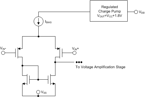
Figure 3: Zero-crossover amplifier architecture
In Figure 4, the black curve describes the output of a traditional rail-to-rail CMOS op amp (OPA340) at the output of a DAC (DAC8830), while the red curve describes the output of a zero-crossover op amp (OPA388) with the same DAC8830. As you can see, the output of the DAC8830 + OPA388 does not suffer from the distortion that is easily visible in the DAC8830 + OPA340 output curve. The High-Precision Reference Design for Buffering a DAC Signal describes this output in greater detail.
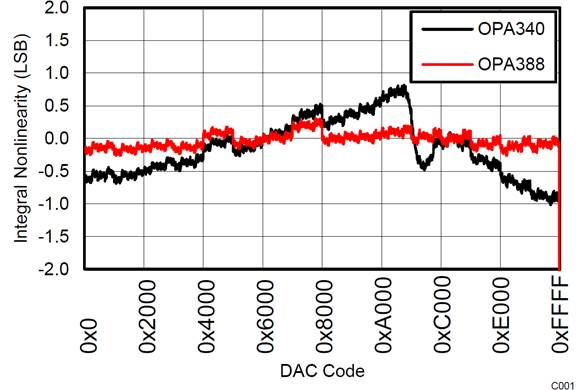
Figure 4: INL comparison of rail-to-rail CMOS OPA340 and zero-crossover OPA388
Let’s put this reference design into perspective and use it in an application such as an MRI machine. An MRI uses a powerful magnetic field to produce detailed 2-D and 3-D pictures of the human body to diagnose and/or monitor several health conditions. Unacceptably distorted signals that exceed the error budget in any way can potentially impair the quality of the images.
The OPA388 is the industry’s first op amp to employ zero-crossover and zero-drift technology. Zero-drift op amps have an internal self-correcting circuit that produces ultra-low input offset voltage (VOS) and near-zero input offset voltage drift over time and temperature (dVOS/dT). The technology also delivers other advantages, including no 1/f noise (flicker noise), low broadband noise (white noise) and low output distortion, which can help increase system reliability in harsh environments. Take a swimming pool for instance – pH pool testers and monitoring systems must withstand changes in the environment’s temperature to correctly determine the deficit or excess of chlorine. Since most pools are placed outside, the environment’s temperature can vary many degrees between a cold winter’s day and a hot summer’s day. Offset voltage will change with temperature deviations, introducing error, so it is crucial to select an op amp with low offset voltage drift to support system reliability through these changes.
To assure high performance, high precision and high accuracy, carefully select parts for your design. Make sure that you understand your system and what you can afford in terms of error, and only then sift through TI’s diverse portfolio for your ultimate solution.
Additional resources
- Download the zero-drift and zero-crossover Tech Notes.
- Visit the OPA388 and DAC8830 datasheets to learn more.
