"V" indicates the enhanced voltage version (see the recommended operating conditions).
"Q" indicates that the device has been tested to automotive specifications.
"D" indicates the SOIC package.
"R" indicates tape&reel.
It is suggested to replace it with the LM2903BIDR.
A Battery Management System (BMS) is responsible for monitoring the health of battery cells by measuring temperature and detecting current leaks or overcurrent conditions. Additionally, the BMS manages voltage levels in individual cells such that energy from discharging, charging, or recovered from regenerative breaking is distributed or sourced evenly to prolong system lifespan.
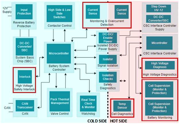
Current Sensing:
It’s important for the current sensing amplifier to be able to monitor current quickly and detect leakage/overcurrent as it occurs. For this a faster transient response is required from amplifiers with a high slew rate and wide bandwidth.
Table 1: Amplifier recommendations for current sensing OPA388-Q1 OPA320-Q1 OPA322-Q1
|
Number of |
Vs min |
Vs max |
GBW typ |
Slew Rate |
Vos max |
|
|
OPAx388-Q1 |
1,2 |
1.8 |
5.5 |
10 |
5 |
0.005 |
|
1,2 |
1.8 |
5.5 |
20 |
10 |
0.15 |
|
|
OPAx322-Q1 |
1,2,4 |
1.8 |
5.5 |
20 |
10 |
2 |
High Voltage Diagnostics:
As the name implies the HV Diagnostics socket requires a high voltage component to measure both voltage and current. The amplifier should also have a wide bandwidth and minimize offset/noise.
Table 2: Amplifier recommendations for high voltage diagnostics OPA192-Q1 OPA197-Q1 TLV197-Q1
|
Number of |
Vs min |
Vs max |
Vos max |
Drift typ |
Vn typ |
|
|
1,2 |
4.5 |
36 |
0.025 |
0.1 |
5.5 |
|
|
1,2,4 |
4.5 |
36 |
0.25 |
.5 |
5.5 |
|
|
TLVx197-Q1 |
1,2,4 |
4.5 |
36 |
0.5 |
1 |
5.5 |
Cell Supervision:
Battery monitoring via cell supervision is necessary for monitoring the balanced distribution of energy among cells and for current faults and leakage. Unlike the current sensing socket here accurate measurements with low offset voltage and drift take priority over speed with no bandwidth requirements.
Table 3: Amplifier recommendations for cell supervision OPA180-Q1 OPA333-Q1 OPA317-Q1
|
Number of |
Vs min |
Vs max |
Vos max |
Drift typ |
IBias typ |
Vn typ |
|
|
1,2 |
1.8 |
5.5 |
0.075 |
0.1 |
250 |
10 |
|
|
1,2 |
1.8 |
5.5 |
0.01 |
0.02 |
70 |
55 |
|
|
OPAx317-Q1 |
1,2 |
1.8 |
5.5 |
0.09 |
0.05 |
200 |
55 |
Temperature Sensing:
Because temperature is not constant throughout the entire system safe designs will include multiple amplifiers connecting thermistors to an ADC or MCU. To address settling issues the ADC-driving amplifier should have low drift over temperature.
Table 4: Amplifier recommendations for cell temperature sensing
|
Number of |
Vs min |
Vs max |
Vos max |
Drift typ |
IBias typ |
Vn typ |
|
|
1,2,4 |
2.2 |
5.5 |
0.025 |
0.32 |
0.2 |
7.5 |
|
|
1,2 |
1.8 |
5.5 |
0.01 |
0.02 |
70 |
55 |
|
|
OPAx317-Q1 |
1,2 |
1.8 |
5.5 |
0.09 |
0.05 |
200 |
55 |
High Voltage Safety Interlock:
Safety Interlock components should be as accurate as possible in their monitoring, Zero-Drift or low-drift components are ideal here. Ideally non-chopper, low-drift amplifiers such as the OPA376-Q1 would be used here as choppers are prone to glitches caused by uneven spikes in the input bias current. This phenomenon can be addressed, however, by matching impedances.
Table 5: Amplifier recommendations for high voltage safety interlock
|
Number of |
Vs min |
Vs max |
Vos max |
Drift typ |
Vn |
|
|
1,2 |
1.8 |
5.5 |
0.01 |
0.02 |
70 |
|
|
1,2,4 |
2.2 |
5.5 |
0.025 |
0.32 |
7.5 |
|
|
OPAx377-Q1 |
1,2,4 |
2.2 |
5.5 |
1 |
0.32 |
7.5 |
For useful resources and additional information, please make sure to check out the following content:
HEV/EV battery management systems explained simply (Technical Article)
Voltage and current sensing in HEV/EV applications (Technical Article)
Understanding current sensing in HEV/EV batteries (Technical Article)
Battery management system (BMS) (Reference Design)
TI Battery Management Video Series (Video Series)
BMS EE Slides (End Equipment Slides)
Part Number: LM2903
Hello,
We need your help to identify the difference in part numbers-LM2903DR, LM2903VQDR, LM2903QD. Are this MPNs compatible to each other.
We appreciate your soonest response.
Thanks & Regards
Pratiksha Walunj
Inverter and Motor Control systems are used in electric vehicles to manipulate an AC signal with pulse width modulation that ultimately controls the vehicle’s DC motor in such a way that steering and acceleration feel smooth to the driver. Other functions of the system include internal sensing and protection features as well as the circuitry behind regenerative braking.
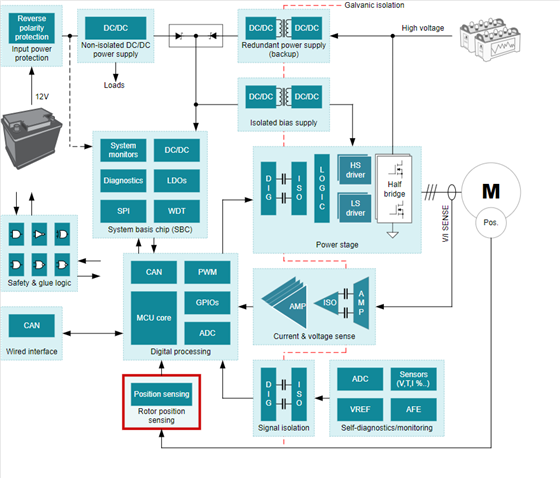
Position sensing:
Key functions of acceleration and steering require the vehicle to “know” the position of moving parts so a circuit must be developed to sense this. Due to the importance of this function many original equipment manufacturers (OEMs) require that this sensing be done in redundancy, two unique solutions preforming the same task but with different components to minimize the chance of component failure at the same time.
Discrete solution:
Position sensing amplifiers require a high current output because of the low impedance found in resolver excitation coils as well as a wide bandwidth and high slew rate to minimize distortion. The majority of amplifiers will not have the current output necessary to fulfill the necessary output current and thus require sinking and sourcing transistors at the output to act as a current pump. There are exceptions to this rule with amplifiers such as the OPA564-Q1, which has current capabilities even greater than what is required for position sensing.
Table 1: Amplifier recommendations for discrete position sensing LMV841-q1 opa197-q1 tlv197-q1
|
Number of |
Vs min |
Vs max |
Output current |
GBW typ |
Slew Rate |
Vos max |
|
|
1,2,4 |
2.7 |
12 |
33 |
4.5 |
2.5 |
0.5 |
|
|
1,2,4 |
4.5 |
36 |
65 |
10 |
20 |
0.25 |
|
|
TLVx197-Q1 |
1,2,4 |
4.5 |
36 |
65 |
10 |
20 |
0.5 |
Integrated Solution:
To fulfill the needs for redundancy TI has created a family of resolver drivers designed to fit perfectly into IMC circuits. The ALM family features wide bandwidths and high output currents resulting in a well-balanced output stage that does not require any additional current boosting circuits. In addition to integrating the additional transistors required in the discrete solution, these devices also include protection features including shutdown, current limit, thermal protection, and are functional safety capable. All this functionality fits into an HTSSOP|14 package potentially reducing board space by as much as 300% compared to a discrete solution.
Table 2: Amplifier recommendations for integrated position sensing alm2402f-q1 alm2403-q1
|
Number of |
Vs min |
Vs max |
Output current |
GBW typ |
Slew Rate |
Vos max |
|
|
2 |
4.5 |
16 |
400 |
2 |
3.4 |
7 |
|
|
2 |
5 |
24 |
450 |
21 |
50 |
25 |
Signal-Processing:
Having moved beyond the previous stage the signal chain continues with post processing. Here, we are amplifying and attenuating the signal, the degree of accuracy required will vary between individual systems but regardless of precision required the key specifications for maintaining signal integrity are offset voltage and offset voltage drift. When choosing amplifiers for HEV/EV functions devices that can be powered by a 12-V rail are usually more desirable as this is the most ubiquitous supply seen in automotive end equipment.
Table 3: Amplifier recommendations for position sensing post-processing Opa192-q1
|
Number of |
Vs min |
Vs max |
Vos max |
Drift typ |
Vn typ |
|
|
1,2 |
4.5 |
36 |
0.025 |
0.1 |
5.5 |
|
|
1,2,4 |
4.5 |
36 |
0.25 |
0.5 |
5.5 |
|
|
TLVx197-Q1 |
1,2,4 |
4.5 |
36 |
0.5 |
1 |
5.5 |
Current/Voltage Sensing:
It’s important for the current sensing amplifier to be able to monitor current quickly and detect leakage/overcurrent as it occurs. To accomplish current monitoring tasks in a timely manner, a faster transient response and quick settling of the output is required from amplifiers with high slew rates and wide bandwidth.
Table 4: Amplifier recommendations for current/voltage sensing opa388-q1 oap320-q1 opa322-q1
|
Number of |
Vs min |
Vs max |
GBW typ |
Slew Rate |
Vos max |
|
|
OPAx388-Q1 |
1,2 |
1.8 |
5.5 |
10 |
5 |
0.005 |
|
1,2 |
1.8 |
5.5 |
20 |
10 |
0.15 |
|
|
OPA322-Q1 |
1,2,4 |
1.8 |
5.5 |
20 |
10 |
2 |
Temperature Sensing:
Temperature sensing has looser requirements than voltage or current as minor temperature variation has significantly less impact on a system than variation in current or voltage. When designing for this function a higher voltage amplifier will enable wider temperature measurements, particularly important as the circuit heats up towards its upper limit. Furthermore, choosing an amplifier with low offset voltage drift will prevent the need for additional calibrations saving time and effort using complex algorithms.
Table 5: Amplifier recommendations for temperature sensing
|
Number of |
Vs min |
Vs max |
Vos max |
Drift typ (µV/°C) |
Vn typ |
|
|
1,2 |
4.5 |
36 |
0.025 |
0.1 |
5.5 |
|
|
1,2,4 |
4.5 |
36 |
0.25 |
0.5 |
5.5 |
|
|
TLVx197-Q1 |
1,2,4 |
4.5 |
36 |
0.5 |
1 |
5.5 |
For useful resources and additional information, please make sure to check out the following content:
Inverter & motor control integrated circuits and reference designs (Reference Design)
Voltage and current sensing in HEV/EV applications (Technical Article)
Understanding current sensing in HEV/EV batteries (Technical Article)
IMC EE Slides (End Equipment Slides)
Applying the ALM2403-Q1 Single-Chip Resolver Solution to Reduce System Costs, and Improve the Reliability and Performance of Automotive and Industrial Applications (Application Note)
Overvoltage Protection of Resolver-Based Circuits (Application Note)
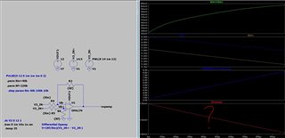
Hi Roi,
what do we see in the scope plot? What are the input signals?
Also, rethink the handling of unused inputs of comparators:
Kai
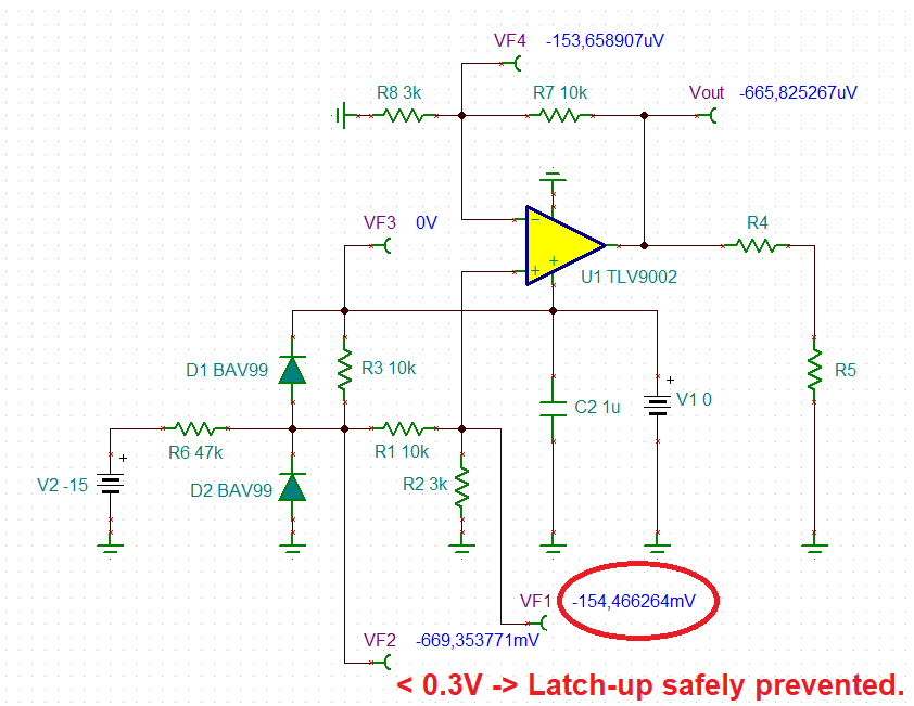
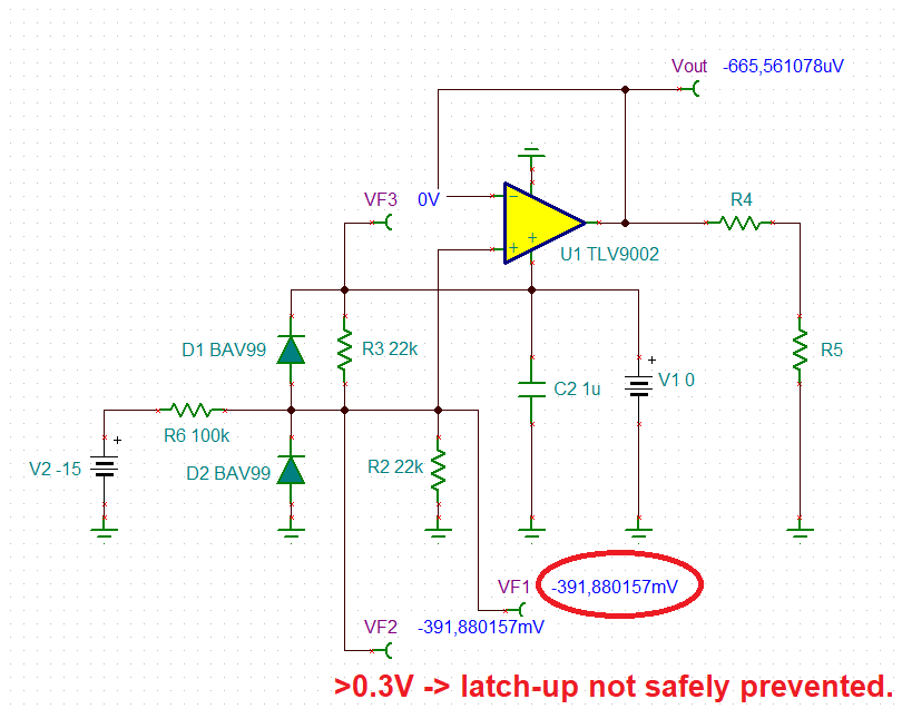
Part Number: OPA170
Hello, i am designing a circuit consisting of OPA170 and hope anyone could answer what's wrong with the opamp (as per item#2). all the supply information as per schematic below. V+ and V- are still lower than the supply.
1. in the below circuit i am using Rf=220k and Rin=100k. the 3rd plot shows the feedback calculation (Rf/Rin)(V3+ - V3-) and the 4th plot is the actual simulation. 3rd plot and 4th plot are identical.
2. in the below circuit i am using Rf=220k and Rin=40k. the 3rd plot shows the feedback calculation (Rf/Rin)(V3+ - V3-) and the 4th plot is the actual simulation. however, the simulation is not as per the calculation