


Part Number: INA301
I’m using INA301 for low-side and high-side current sensing on a single sense resistor using the following topology :
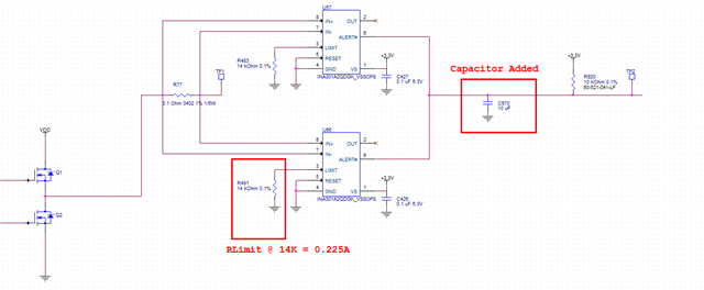
Issue #1
—It works fine in theory but there’s a major issue. The Mosfets switching from sinking to sourcing generate ground bouncing/noise that affects the differential inputs of the INA301, asserting the alarm output by doing so. The data sheet mentions that by adding an input filtering it could potentially compensate for that kind of glitch. It didn’t work out as expected with that method. However, by adding a bypass capacitor directly on the alarm output , the glitch was still present on the differential inputs but not triggering the said alarm. Is there any recommendations for this specific design you could provide me with. Do you see any issues that could occur by adding the bypass capacitor, besides delaying by a small margin the alarm output? The said bypass capacitor is in the magnitude of 10 uF and the glitch is about 5 us in High-side and 1 us in Low-side. TP 1 represents where the load is located and TP 2 represents the alarm output.
Potential workaround
— The current design is using INA301A2, but could potentially be changed to INA301A1 for higher differential input voltage.
Note that the switching noise/bouncing asserts the alarm on the INA301A2 using an 2A current limit with a 0.03 mOhms sense resistor. I’m assuming that by changing the sense resistor to an higher value and using INA301A1 with a higher differential voltage/lower gain , the “false” alarm assertion would be more or less an issue. Is my assumption correct?
See the specifications below :
-Current limit, 0.225A to 2.1A
-Rsense = 0.03 ohms
-high side to low side switching : approx 580 ns
Regards,
