This thread has been locked.

If you have a related question, please click the "Ask a related question" button in the top right corner. The newly created question will be automatically linked to this question.

LM8272: Difficulty attempting to drive a power MOSFET with an opamp (analog signal)

Part Number: LM8272
Other Parts Discussed in Thread: LM7322, LM7332, OPA1678

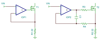
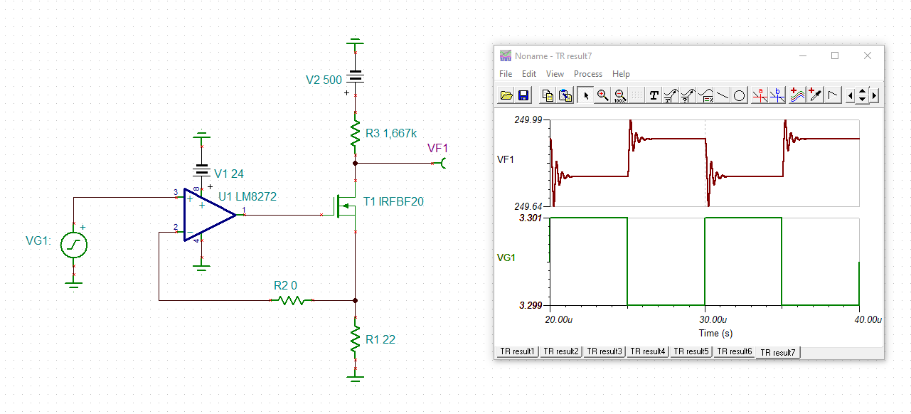
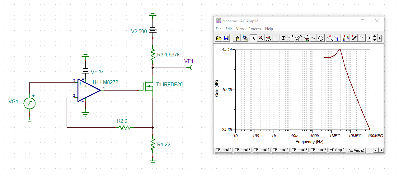
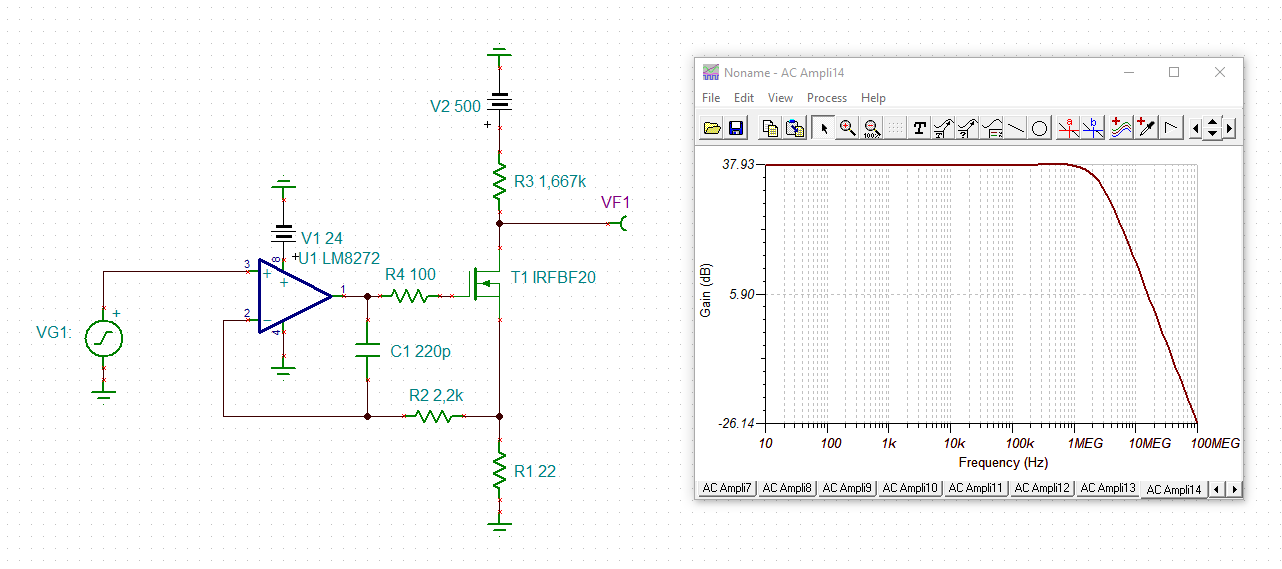
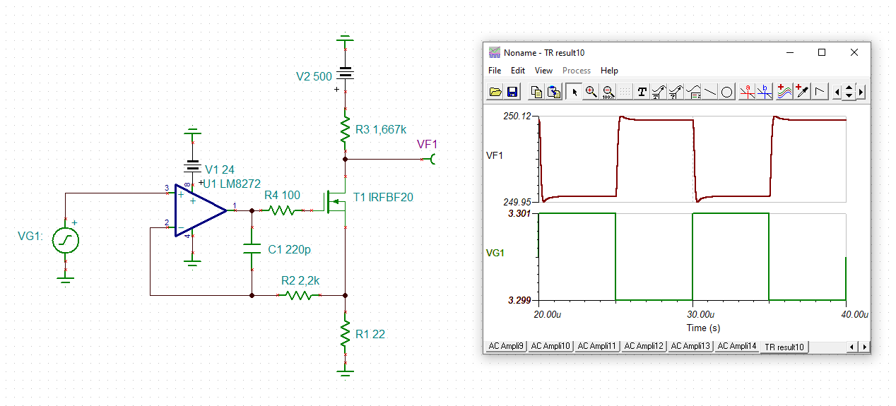
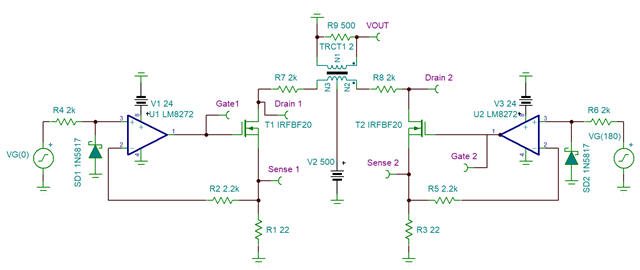
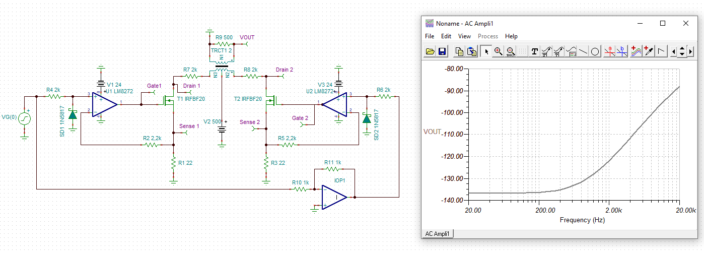
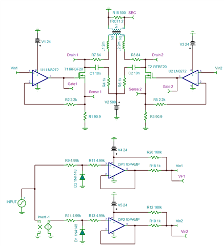
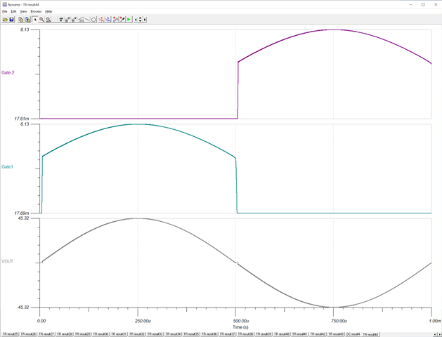
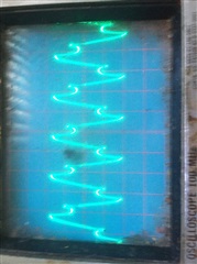
So I have an application where (don't laugh TOO hard) I'm actually trying to use a power MOSFET to replace an actual vacuum tube power pentode, the "class" of the drive is about 500 volt at .15 amp. I selected the LM8272 because my original "attempt" used a garden-variety dual opamp and I wanted something that would "more or less" fit the socket (as adapted). The MOSFET is an IRFBG20F, it's wired so the opamp is configuring the MOSFETs as current sources and tries to "persuade" the transistor to generate a peak of 3.3 volts across 22 ohms in the source return. The problem is the maximum output I get before the waveform "goes wobbly" (has all manner of extra trash on it) is at least 13X less than it ought to be capable of. Now I notice the LM8272 doesn't claim to have been designed to drive power MOSFETs, just to be stable regardless of the amount of capacitance in the load. Should I have used an LM7332 or LM7322 instead, their data sheets appear to say it's OK in this type of service? What's the difference between these parts that I should notice? What else would be misbehaving here? (I'm "not a big fan" of SPICE because I usually don't find the models to be accurate enough to be revealing with "bleeding edge" parts and configurations, and I don't think I have models for even the opamps let alone the MOSFET, but rather than spending weeks JUST to get a simulation to reproduce an instability that I can already see, what's throwing me here anyway is the data sheets' insistence that these devices are "unconditionally stable" with a highly capacitive load, "maybe except for" - except for WHAT??) Are there other "candidates" for this service, maybe the OP275 (not "unlimited" cap but to 1 nF and not "designed to drive" MOSFETs), are there others? (The load can be somewhat inductive.)

  • Hello Jeffery,

    Driving a FET is a little different then adding a FET into the feedback loop. If the long loop, has phase lag then stability of the loop will be an issue.

    Is your circuit closer to left or right schematic?

    Do you have waveforms to share?

  • It's definitely the left side. The input happens to be AC coupled so there's an input resistor that returns to where you show ground (and there happens to be a small zener down to the real ground for biasing, that's actually at the opamp supply's negative rail because I'm working with an existing circuit). There's a pair of them driven off opposite ends of a phase inverter, but the "crud" appears to be quite symmetric and highly dependent on input amplitude. The application needs a fair amount of bandwidth so the version on the right would appear to be unworkable except maybe as an experiment.

  • Hi Jeffrey,

    can you show a schematic? And what bandwidth do you need?

    Kai

  • Hi Jeffrey,

    like this?

    jeffrey_lm8272.TSC

    Kai

  • And the frequency response:

    Kai

  • Well gee Mr. Kai, this would all be really wonderful if it had anything to do with what I'm trying to do. You see each of these "current sources" I'm building is connected to either end of an audio output transformer, about 4K ohms center-tapped (the center tap is where the 475 volt supply connects). I have no trouble generating lots of "output voltage" so long as I'm only looking at an "unloaded" transformer, both the input and output side look really nice. But as soon as I "connect a test load" to the secondary so I'm actually asking the MOSFETs to supply actual current, waveforms on BOTH sides of the transformer tell me it's not prepared to supply any REAL current. Now this "instability" is present even when I use my "simple minded" left-side circuit that doesn't introduce any additional poles that I have to worry about (not that I don't appreciate the cleverness of the circuit you're showing but I may need to introduce my own "network" to deal with the characteristics that the transformer introduces into the circuit like leakage inductance). And this "defective output transformer" works just FINE when I plug the vacuum tubes in instead. And I have always heard that a "power pentode" vacuum tube is modeled as a voltage-controlled current source. (I of course am not attempting to "scale" the opamp input voltage the same as the vacuum tube.) And of course your circuit is looking at voltage generated across a load RESISTOR which is a totally different issue. So how can I use a power MOSFET to drive substantial current into a transformer, do you have any ideas? (No I don't have a schematic of this yet.)

  • Jeffery,

    How certain are you that the vacuum tube solution provides current drive. I think more possible that it provides voltage drive to the transformer. Do you have two pentodes, one per transformer primary end?  Having the tube circuit schematic will make it easier to convert to FET.  My first job was fixing tube television sets. I never converted one to FET before.

  • Take a look at the chart labeled "plate characteristics", you pick a grid voltage, it maps nicely to plate current off the left axis:

    https://www.telefunken-elektroakustik.com/wp-content/uploads/2017/06/6L6GC-TK-Tube-Data-Sheet.pdf

    Yes you have one tube for each end. I currently have a 10K input resistor on the non-inverting inputs, there is some input bias current so at "idle" that input is about 25 millivolts over the return which is practically zero idle current, and the two sides are consistently driven out of phase. You want to drive current anyway or else the load would be lagging by the amount of leakage inductance in the transformer. The confusing part is my scope photos aren't revealing any high-frequency parasitic components (it's all "in-band"), I tend to believe the opamps aren't being destabilized by the gate capacitance anyway. As far as the product concept the actual replacement of physical tubes was "only one feature" but it does substantially drop power consumption at idle (about 21 watts per tube). Now if a more sophisticated component topology, maybe an extra opamp, would solve the problem that would be fine, but the way things are it's kind of difficult to identify the issue, and the last time I checked SPICE models for transformers were either totally absent or unreliable. That's why I was interested why these alternate opamp types say they're designed to drive MOSFET gates and this one didn't? (Getting parts here while we're still facing COVID-imposed delays, including long ship delays, is certainly annoying, I'm just looking for guidance if you have it.)

  • Jeffery,

    I had better simulation luck driving the gate directly. This has some crossover delay. R7 and R8 represent the winding resistance. I have simple clamp diodes on the input to block the opposite phase. A more dedicated phase splitter would do a better job. Would you mind if there was a static off current so the turned off driver can turn back on quicker?

    jeffrey_lm8272_3.TSC

  • Jeffery,

    Lastly, what is the maximum frequency needed?

  • I appreciate your trying Ron, frankly I just didn't think this was all that "weird" of an application but I completely understand, I had sort of thought if some of these devices are marketed as "capable of" driving MOSFET gates that maybe this was close to what was intended. I measured the DCR on the transformer primary and it's about 84 ohms per side, I also measured the "open-circuit" inductance END-TO-END on the primary and it's up around 19 henrys, whereas under load it drops to about 2.1 henrys (you can make the secondary anything you like), this is with a component meter and unfortunately I can't tell you at what frequency the measurement was taken. I'm impressed that you have a SPICE transformer model at all and I have no idea whether you can successfully "drop in" these values. Right now I've ordered at least two each of all the opamp types I mentioned (Digikey "blew it" and put the 7322's on backorder after telling me they had them so the order went to Mouser). Probably before the day is out I will try modifying the circuit to allow me to put an IXTP08N100P in to replace the IRFBG20 on one side (since it's probably the only credible alternative), it's about half the gate capacitance as it's about half the current rating, that may tell me quite a bit. One of the considerations of driving MOSFET gates is the capacitance varies substantially with the drive voltage, I believe the tend is it drops as the drive increases but don't count on me knowing what I'm talking about (that's why they measure it at 25 volts or something). You really don't have to work on the SPICE aspect if you don't want to, I've tried using it for motor drive before (high inductance among other things) and it turns out it's not really the "Swiss Army knife" it's touted to be, all I really expect to learn from TI is to get a little better handle on the "unlimited capacitive load drive" opamp versus the "dynamic capacitance load" gate input - the irresistible force meets the immovable object! And my hat's off to you for going into all this detail, that's the spirit!

  • Somewhere between 15 and 20 kilohertz would be great.

  • To be a little more precise, look at Figure 5 in the following PDF:

    https://www.vishay.com/docs/91123/sihbg20.pdf

    The charge needed to move up and down that curve has to come from SOMEWHERE, isn't that an additional strain on the opamp output? (Does the SPICE model completely simulate that curve for this part? Consider me a skeptic.) Should I expect better results from these other part #s which CLAIM to perform well in this service? Do I need to go to a discrete "output booster" to add onto a more "standard" opamp?

  • Jeffery,

    20kHz for 2.1H inductor is 264k ohms of impedance. That's just 2mA AC even with 500V drive.

    The stability of the output drive will be the part that will need most of the tweaking to get right. The circuit I last suggested worked fine with the ideal transformer and resistive load. With a more complex transformer and load mode, it might not be stable. Even with a powerful gate driver, stability may be an issue.  Increasing the sense resistor could help (what is the peak current expected?)

    Instead of the input diode clamp, these half wave rectifiers will pass just half of the signal to each side. There is a small pull-up at the end to keep the FETS lightly conducting in the off mode to make the next turn on cleaner. 

    The inverter is just a block here. This can be AC coupled for the main input if the minimum frequency is known.  

  • Can't use even precision rectifiers, they introduce distortion. What I did was I AC coupled a symmetric signal to the output stage, the 22 ohm resistors returned through a 7.5 volt zener to the NEGATIVE opamp rail and everything runs with plenty of headroom.

    You caught me in one mistake though, when I measured the "leakage inductance" I accidentally had the load connected, it was NOT a dead short. When I did short it the leakage inductance dropped to 20.3 millihenries or about a hundredth of what I previously reported! Sorry for the confusion.

    Those gate drivers are only for digital application, I checked.

    Give me a few hours, don't want to close it out yet but I seem to be looking for some manner of miswire, the "static" voltages all seem OK but some of the waveforms look a bit "off". (I have it coming, there's seven opamps total for processing, and it may look odd but this DOES have commercial potential, I'd buy my transistors from you guys too if you had anything in this operating class.) It COULD be that after I get this "making sense" the new opamps resolve the remaining issues but I'm not quite there yet. Do you know if there's anything the LM7322/7332 has or does better than the 8272, besides being offered in a more reasonable footprint?

  • Hi Ron,

    would this be the frequency response?

    Kai

  • Hi Ron and Kai,

    Let me first reference a chart for my "alternate" transistor, then I'll tell you what I currently know. Now earlier I referenced the chart for capacitance, I mentioned Figure 5 on that data sheet. On the following data sheet I want to call your attention to Figure 11 which is analogous for the other transistor:

    https://www.littelfuse.com/~/media/electronics/datasheets/discrete_mosfets/littelfuse_discrete_mosfets_n-channel_standard_ixt_08n100p_datasheet.pdf.pdf

    Now I was up rather late lat night for a number of reasons. It turned out with the network I was using there was what in my industry used to be called a "gain structure" problem, I wound up with about 8 db of loss in my network where I wasn't told to expect any, unfortunately I use that 3 times so basically I'm down maybe 24 db. So the reason I wasn't getting high levels of current into the load was that I wasn't asking for the right amount of it. It's a prototype, no problem. It's just not demanding enough current yet.

    The BIG problem is still why were those "giant chunks" missing from the output waveform (even when it was "scaled down" a bit)? Well look at how nonlinear the capacitance vs. gate voltage plot is, for EITHER transistor. There's your answer! As the total charge varies, the gate current changes WILDLY, this changes the voltage across the source resisor and effectively "modulates" the current, in a highly nonlinear fashion. So I need either a) to find a transistor in this class that doesn't have this effect, or b) find an opamp that can drive the transistor steadily without this phenomenon, or c) come up with a modification to the circuit that isn't nearly as susceptible to this effect. I suppose "in theory" one could try and "swamp out" the change in gate cap by putting a LARGE cap across the gate? I'm not a fan of this approach, after all this IS audio, and I keep thinking there HAS t be a device that is "more immune from" this effect, can you help me either find it or build it?

  • Maybe I ought to be considering an IGBT instead of a MOSFET, on the basis that the overall gate capacitance (therefore the gate charge delta) that I'm having to drive looks like it might be lower? It seems REALLY weird trying to operate one of these devices in the linear region, also not sure how fast the PNP component turns off, but they do have a robust power dissipation rating (just an idea, if it doesn't make sense just ignore it), I don't have any in stock to try of course:

    https://www.infineon.com/dgdl/Infineon-IHW15N120E1-DS-v02_01-EN.pdf?fileId=5546d4625696ed760156a2b608492129

  • Jeffery,

    I know the original quest was to replace tubes. Your tube is good for hundreds of volts but only one to maybe two hundred miliamperes. So often a transformer is used to convert the high voltage & low current into a lower voltage at much higher current. Is this the case? If yes,then maybe it's time to ditch the transformer too.

    The half wave rectifier I presented previously does glitch a little at cross over but it was accurate until I placed a pull up load at the output. It definitely didn't like that. So I made a half wave that just cuts off the other half. This is old school but it works better. All that is needed is a rail to rail output op amp that resists phase reversal.  

    I haven't used IGBT personally but I haven't seen them used for a linear application.

    Anyway here is my latest revision. I added 84 ohms and 2mH to the ideal transformer to be closer to your load.Then I added a RC snubber that keeps it from oscillating.

    I don't know if this works with your load. 

    jeffrey_lm8272_6.TSC

    This one does show gain on a small signal gain analysis.

  • Kai,

    would this be the frequency response?

    The small signal gain would be very low as your plot shows. Large signal, such as 1kHz 2Vp had a gain of 22.7 (+27dB).

    Notice the crossover delay near 500us. This is why I added the half wave rectifier and signal offset +14mV (in newer versions). This creates a static current in the off phase time that is about 14mV/22 ohms = 636uA. The idea is to keep the minimum gate voltage high instead of dropping to zero. The time is takes for gate to go from 0V to VT and back makes it terrible for small signal analysis.

  • The whole idea is this has to be a "drop-in" replacement at the tube socket level, there can be no access to any resource that is not available at a socket pin. I mean we can discuss theoretical "options" but in the end this is what I'm committed to doing.

    Anyway you are apparently "content" with a design that for me is showing HIDEOUS amounts of distortion on the oscilloscope, it's so huge you can't even assign a percentage to it, you can hardly recognize that the waveform is even a sine wave! This results from the "artifact" that as the opamp constructively and destructively generates gate current, that current appears across the source resistor which is responsible for "programming" the amount of current that goes through the drain pin. Here's what it looks like, unfortunately it's rotated:

    Now the waveform you are looking at is measured across the load resistor at the secondary of the transformer. This is exactly why I said at the beginning of this entire exercise that I'm frankly "not too keen on" using SPICE as a means of assessing "what's going on" because it likely doesn't attempt to model the nonlinear gate capacitance AT ALL! If I take the load resistor OFF then yes the waveform gets a lot larger and cleaner but I mean this waveform you're looking at is only about 70 millivolts RMS, there is NO REAL POWER being generated. And to get here the waveform went through a few 12AX7 tubes in the "target amplifier" and a few OPA1678's running at unity gain. This is using the original "designated" circuit. I notice that the "notch" it "takes out of" the sine wave always happens EXACTLY as the current is coming down, which makes me think the LM8272 is having more trouble sinking current; this is why I was asking if you knew whether any of the three "alternate" parts would be a better fit (I guess one of the numbers I presented is Analog/LTC not you). I CERTAINLY thought I was going to find a little better knowledge about the suitability of your parts for an audio application! I suppose you could either return the gate current through the source somehow or measure the current through the source (floating at up to 475 volts), you see even though the parts cost may not be high none if these solutions is exactly "simple" to complete a design for.

    Anyway this is anything but a "theoretical" issue. I have a few customers waiting on me to finish the design and layout, panelize and etch PCBs and do SMD assembly. If inherently defective SPICE models  is "the best you can do" then I'd better start panicking sooner than later!

  • I meant "...measure the current through the DRAIN..." of course, so sorry...

  • Hi Jeffrey,

    I don't think that it has to do with nonlinear gate capacitance or defective Spice models.

    It's just that a real transformer contains an inductance and a winding capacitance. Being in parallel they both form a sharp resonance of very high impedance. A current source will result in a sharp voltage spike across the transfomer resosance.

    I don't think that a current source will do the trick. And I don't think that a pentode works as a current source. Of course, the anode current can be controlled by the gate voltage. But that does not mean that it's working like a current source.

    Kai

  • Actually the CORRECT answer is to avoid the gate capacitance entirely and replace the MOSFET with a "flyback transistor" (NTE2679 or MJW18020 are representative part #s). These are "technologically obsolete" high voltage NPNs but you can go on the Chinese websites and if you have the correct # they'll sell them to you 5 for $5 all day long. The beta on these parts isn't very high so they need some current from the opamp but there's very little voltage swing needed. Will order soon and test next week. Hope you learned something useful. Thanks anyway. 

  • Good luck Relaxed

    Kai