Because of the Thanksgiving holiday in the U.S., TI E2E™ design support forum responses may be delayed from November 25 through December 2. Thank you for your patience.

This thread has been locked.

If you have a related question, please click the "Ask a related question" button in the top right corner. The newly created question will be automatically linked to this question.

THS3062: Strange behavior from opamp at non-inverting input

Part Number: THS3062
Other Parts Discussed in Thread: THS3215, THS3217, OPA838

I have the THS3062 configured as an instrumentation op-amp as shown below:
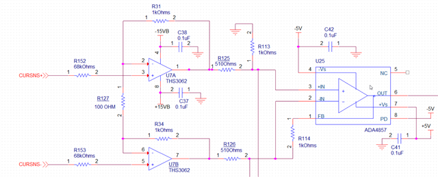
The currsns+ and currsns- inputs are a ~2Vp sinewaves at 13.56MHz..  I expect to see a slightly smaller, off-phase version of those signals at pins 3 and 5.   Instead, I see what appears to be a 0.45V DC signal.  What could be going on?  pins 3 and 5 are high impedance inputs.  I've verified power, layout, component values, population options, etc on the board.  I'm stumped.  Any suggestions as to what may be going on?

Simulation of circuitry works well.

Thanks,

Jorge

  • Well Jorge, 

    Why do you have such high series input R's. The bias current can be quite high into the V+ input, might not be in the model - try reducing those 68k to 1kohm and see if works better. 

  • Hi Michael, thank you.


    I tried it, and it improved but it is still not what I expect.  The 2Vp signal gets reduced to about 880mV.   Perhaps that is right, given the input capacitance  of the op-amp –I ‘ll have to look – but it seems excessive.


    So, if the bias currents are 6uA (typ per datasheet), with 68kohms, I should  have an offset of 0.4V. So bias currents alone should not be the reason the input signal at the noninverting signal is not what I expected.  They would provide an offset, to the input signal.


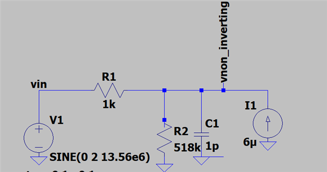
    If I model that input of the opamp as a shown below:


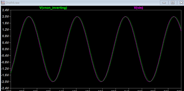
    With the 1k resistor in series, I still get:


    So the 880mV I’m measuring on the board is not quite right.


    It’s quite strange.  These op-amps get hot too –apparently others on the forum noticed that too!


    Thank you again for your input.  I think 68k is too much, but there may still be something else lurking.


    Jorge

  • So Yes, at about 10mA each and 30V supplies, that is about 600mW just for quiescent power and you would feel that. 

    So you do have quite a lot of differential gain (21) - any chance those 2Vpp inputs are out of phase and you are overdriving the outputs

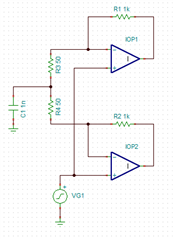
    Another kind of long shot is diff I/O stage sometimes runs into CM stability issue. Not normally with CFA with Rf too high, but a test would be to split the 100ohm gain element into two 50ohm elements and take their center point to ground though say a 10nF cap. That will be invisible to the desired diff signal but raise the CM gain quite a bit at higher freq. 

  • I didn't really fill in some gaps yesterday, but if you are seeing what is essentially a bizarre input impedance (which must be the case for the attenuation you are seeing) a part that is not operating in its linear region might be the cause. If the output is banging into the rails, some of these parts then feedback to shift the input stage characteristics. If are part is oscillating CM wise, again that can get back into the input stage through either thermal mechanisms or operating point issues. All bets are off if the part has these issues overlaying what you are looking for - not that it does, just guessing at this point. 

  • Hi Jorge,

    strange is only how you torture this OPAmp Relaxed

    The THS3062 is a 300MHz current feedback OPAmp with a slew rate of 7000V/µs. You cannot treat such a racehorse like a standard 1MHz OPAmp. The 68k input resistors are way too high for the 40µA input bias currents. This looks totally absurd. And you heavily overdrive the output with the combination of too high input signal and too high gain. This will not work and the DC offset voltage shift is just what you are used to seeing when torturing a HF-OPAmp in such a way.

    Kai

  • Well Kai you are right of course, but you should read some of the earlier replies. 

    I will say in the early Comlinear days when folks blew up our $50 hybrids like the CLC220 and CLC203 etc, it kind of bothered us, but kind of didn't as they just needed to buy more. 

  • I always read all your replies Relaxed

    Kai

  • Hi Kai,


    My absurd circuit works very well in simulation – I was unaware that the models for that op-amp have such low fidelity to the real device.

    I agree that the 68K is high –but the bias currents should not be an issue.  They should  add a  DC offset at the non-inverting input, and at 68K and 40uA, that amounts to a 2V offset which is well within the common mode voltage of the op amp.  I’m powering the op-amp from +/-15V rails.


    Frequency response is a different issue, since at 13.56MHz the 68K (actually 68k||518K) and the 1pf , the attenuation at the non-inverting input is 0.12.  So, that was my bad.  It still doesn’t not explain why when I then change the resistor to 1k, I don’t get the expect Vin*.90 at the input of the op amp.


    Wrt to driving the opamp too hard….not sure what you’re talking about.  The each op-amp is seeing a 2Vp sinewave.  And in fact, I should be able to drive up as high as 8 or 9 volts  if I recall from the specs on this op-amp.  In the configuration as a difference instrumentation amplifier, the signal I’m amplifying with the gain of that circuit is about 50mV. Hence the large overall gain.  But, please do illuminate me.  How do you suggest I amplify the voltage difference across a 0.2ohm resistor? 


    I appreciate the help.  But, in the future, before calling something absurd, I would recommend you first seek to understand what I’m trying to do.  It may still be absurd in the end, but I don’t really need you telling me that.  You can provide an explanation as to why it won't work, and give me some pointers without that comment.  


    Jorge

  • Hi Jorge,

        Definitely a head scratcher. I agree with Michaels comments that in case of phase delays between the two halves you could potentially overdrive the output leading to non-linear behavior which could then result in the attenuated signal. What does each individual output and the differential output look like on a scope with the 1k series resistors?

    What is the capacitance of your scope probe?

    Another thing Michael brought up is raising the CM gain if you can use two 50-ohm resistors for Rg and tap the center point with a cap to GND.

    Finally I am curious as to what the amplifier does if you put in a differential signal. You will have to reduce the signal on each half to around 1Vpp . Does this result in an attenuated signal at the non-inverting pin?

    Thanks,

    Samir

  • Hey Jorge, 

    We will resolve your immediate issue from what is obviously a hardware test at this time. But I was looking at your full schematic again (essentially pulling out a small signal on large differential signal, gaining it up, and running out single ended) and you perhaps should be aware of an alternate solution. 

    We were doing these parts for AWG signal paths, but might be interesting for this if you ever re-design. 

    The THS3215 is probably adequate (the THS3217 is faster) and comprises a fixed gain front end differencing amp with fixed gain of two. The 2nd stage OPS can be set up for quite high gain of that differenced residue if need be (being a CFA like the THS3062). It is not as high a supply voltage, but I can't tell yet you really need +/-15V supplies. 

  • Hi Jorge,

    if you had an OPAmp with a JFET or CMOS input stage the source resistance (R152, R153) wouldn't play an all too big role. The input bias current was low and the input capacitance would act as a low pass filter in combination with the source resistance.

    But here you have an input stage with a BJT which needs a relevant static and dynamic (!) base current to operate well. With a too high source resistance you will throttle the input stage and ruin the HF operating point.

    The THS3062 is optimized for impedances of <75R seen from the +input to signal ground. All the data shown in the electrical characteristics have been gained with this test condition. And you can see this from the maximum input bias current specification as well: 40µA x 75R = 3mV. This is in the same range as the 4.5mV maximum input offset voltage of THS3062. Maybe you can increase the source impedance by a factor of ten resulting in some hundreds of Ohm. But then you are still a light year away from 68k.

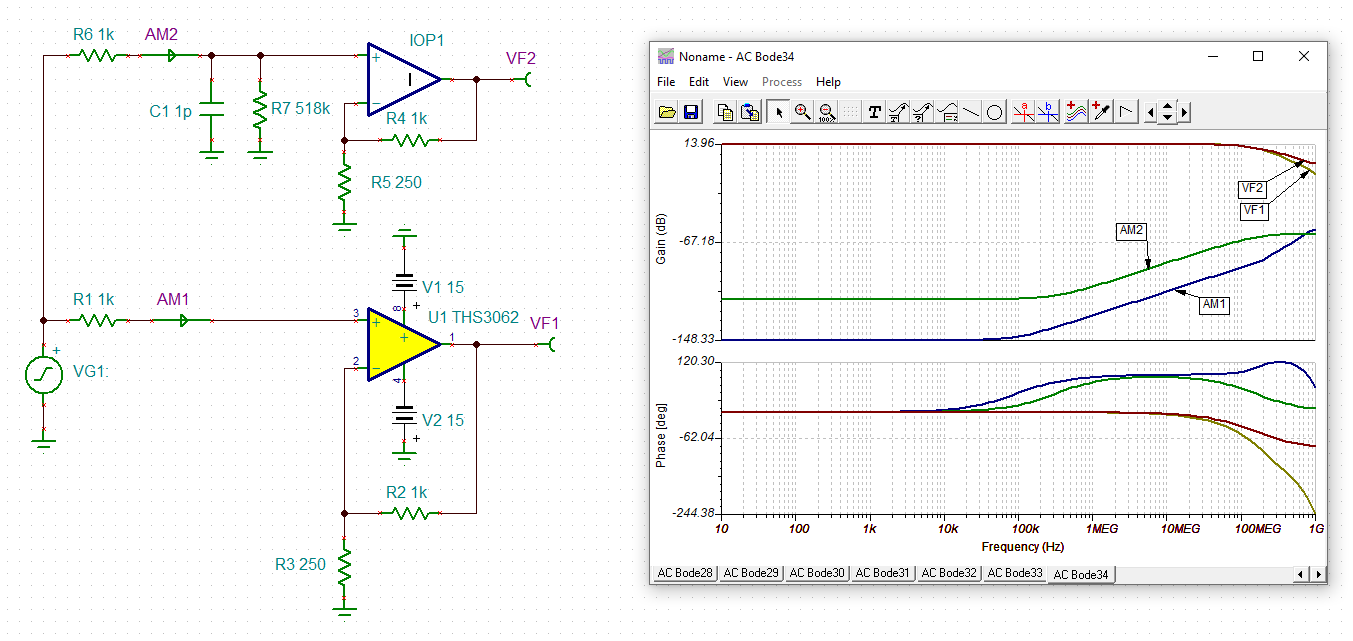
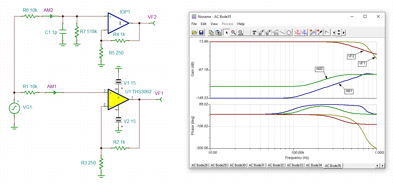
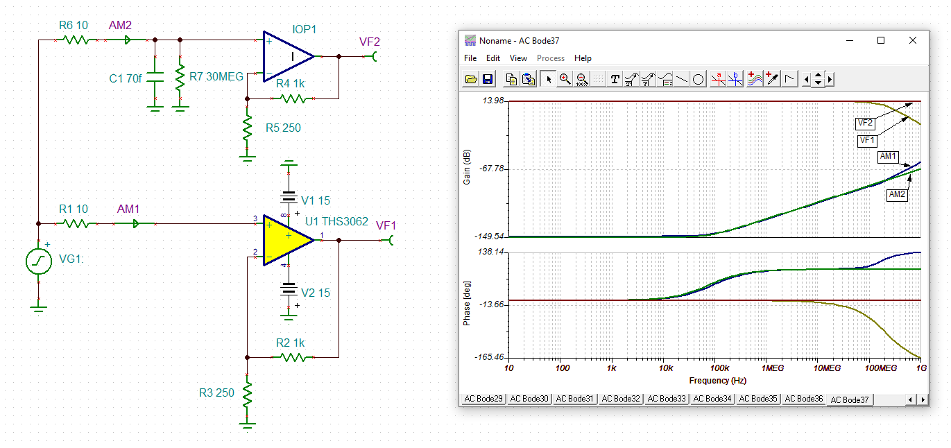
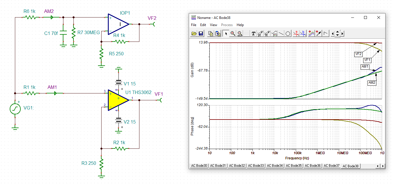
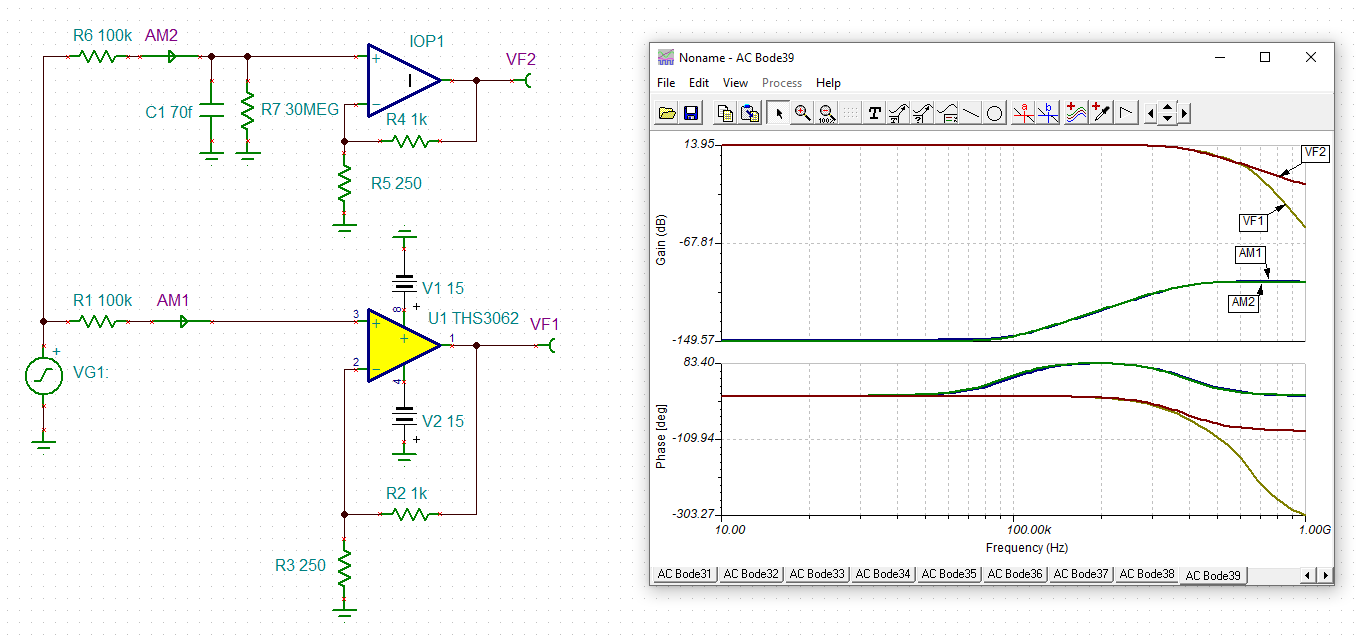
    Unfortunately the SPICE model of THS3062 is not ideal. The input capacitance and input resistance are not modelled properly and I think the dynamic input current isn't correctly modelled either. See the following simulation where I compare the THS3062 with an ideal OPAmp added by the specified input capacitance and input resistance of THS3062:

    70fF and 30M gives a way better fit than 1pF and 518k:

    jorge_ths3062.TSC

    So, the input stage of THS3062 isn't properly modelled and the simulation will not show you what's really going on with a 68k source resistance!

    Having said this, in a standard circuit with low source impedance the model is working well Relaxed

    Kai

  • Thank you again for your help.


    It is a shame that the model is that far off.  I have the whole circuit simulated and working well, and my expectation was that minor tweaks would be necessary in the HW to make it work properly,  not that “it wouldn’t work”.

    I’m not set on 68K- I just wanted a high impedance to avoid loading the circuit under test - 1k or lower might work fine—I just need to work through it. 


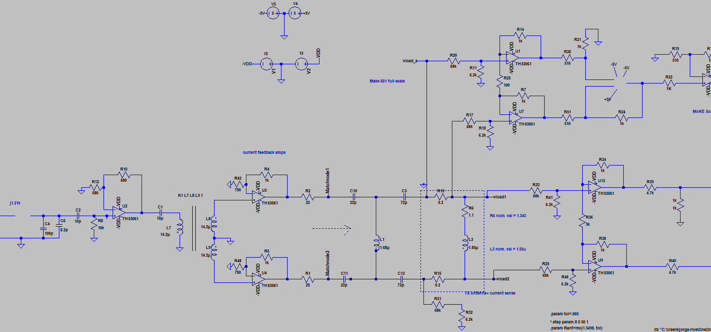
    The portion of the circuitry I shared is the portion that amplifies the voltage drop across a sense resistor. Attached is the complete circuit (it’s in LTSpice, though ; I’m included the netlist too).   I start up from a 13.56MHz oscillator, filter out the fundamental, and convert the signal to a balanced signal to differentially drive a load (coil – similar to NFC antenna).  I then monitor the current and the voltage drop across the load to determine the delta impedance change of the coin in the presence of a metal or capacitive object.


    the differential voltage across the sense resistor is very small, hence the large gain in the instrumentation amp.  ON the voltage side, across the load, the differential voltage is large, so the signal conditioning change is less stringent.  The voltage across the sense resistor (current), and the voltage sensed across the load are then fed to a 2_channel, simultaneous sampling ADCs (at 40MHz), so that the impedance of the load (or the delta impedance) can be calculated.oscillator_PA_balun_match_to_1_1+j158.zip

  • Hi Samir, I will have to get back to you on that.  I will measure these tomorrow and share in this post.

    I don't understand the raisin the CM gain like you suggested.  Can you expand on that a little --perhaps a diagram to make sure I understand what you're suggesting?

    The phase difference between the signals is minimal, since they are the same signal, on either side of a 200mohm resistor.  The difference is small --about 50mV.

  • Kai,

    Can you explain what I'm seeing with the AM1 and AM2 signals?  Why isn't it -0.0289, for example, for the case where R6 = 100k, and C1 and R7 are 70fF and 30Meg, respectively?  At DC, shouldn't the gain plot reflect just the divider, ie, 20*log10(30/(30+.1))?  

    Thanks

  • So Jorge, 

    As you get further into explaining this, I do wonder why you are using the very high slew rate Dual CFA for the front end. 

    Just as a guess, I would have used two OPA838 where that datasheet is where I talk about CM loop oscillations back in the apps text. Doesn't apply as much to your circuit but would to the OPA838 - I actually ran into applying the OPA838 to a Google project, 

    So keep in mind, looking into the V+ inputs of the THS3062 is already very high impedance, you don't need to raise with external (noisy) resistors. in series. 

  • Hi Michael,

    When I first started looking at this, I was running into BW and what I thought were slew rate issues.  I started out with high speed voltage feedback op-amps, but the distortion and non-linearities observed the output drove me to the CF types.  

    Yes, I can 0-ohm jumper the input resistors into the noninverting inputs of the op-amp.  They were there for isolation, knowing that I would revisit their values as I brought the board up.  However, I will need some resistance, as I need to bring the signals down to the CM range of the op-amp.  The signals at the input can be as high as 50V. (another reason for the high slew rate requirement of the op-amp).

    Are you able to see the circuitry I uploaded in a response to Kai?   

  • I wouldn't make those series R any lower than 100ohm - there are many layers to what goes on with these CFA input stages, and inductive source impedance (traces) by themselves have caused self oscillation in the input emmiter followers. keeping some R there usually removes that as a possible perturbation. 

    I have not been looking at this one, working on some other queries. 

  • Hi Jorge,

    It is a shame that the model is that far off.

    Yes, that's annoying sometimes. But better than nothing.

    I’m not set on 68K- I just wanted a high impedance to avoid loading the circuit under test - 1k or lower might work fine—I just need to work through it.

    Yes, I understand, you wanted to isolate the antenna from the OPAmp's input impedance. I would do the same.

    Can you explain what I'm seeing with the AM1 and AM2 signals?  Why isn't it -0.0289, for example, for the case where R6 = 100k, and C1 and R7 are 70fF and 30Meg, respectively?  At DC, shouldn't the gain plot reflect just the divider, ie, 20*log10(30/(30+.1))?  

    The AM1 and AM2 signals are referenced to the input signal VG1 and the ratio of AM1rms / VG1rms is formed. If the VG1rms=1V and AM1 is 1V / 30.1Meg = 33.22591nArms at DC, then this means a "gain" of 20 x log (33.22591n / 1) = -149.57dB. "log" is the base-10-logarithm here.

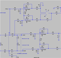
    Here is a snippet from your LTSpice schematic:

    Kai

  • Hi Jorge,

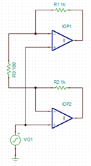
    In the circuit below when the same signal is applied to the inputs of both amplifiers, there is 0V difference on both sides of the 100-ohm resistor. The input signal (VG) is therefore reproduced at the outputs of both amplifiers...therefore the signal gain is 1. As you are aware that a G=1V/V configuration has lower phase margin vs a higher gain configuration.

    Now if you used the circuit below for example, at mid-frequencies the circuit works just as above, however at high frequencies (near the amplifiers crossover region which is where stability matters) you have a low impedance to GND so that decouples each individual amplifiers feedback loop and results in a higher noise gain circuit. Now a current feedback amplifiers (CFB) stability is based on the value of feedback resistance, however there is a secondary noise gain effect. The feedback factor of a CFB =  (Rf + Ri * Noise Gain). Please check out this video for more information on CFB compensation.

    By increasing the high-frequency noise gain you improve the phase margin subsequently improving stability. Hope this helps/

  • looks like some of the symbols didn't come through.....let me know if you need these --I thought I included them in the zip file, but maybe I left them off unintentionally

  • good stuff.  Let me look at the video.  Thank you.

  • So Jorge, looking at what Kai put in from LTSpice, lot going on here, but is your question related to these two stages?

    That is close to what you originally put in, but it does show an attenuation into the V+ node? So what are exactly talking about here? 

    Also, I have been assuming you have this built up and probing. A lot of my comments have been implying a possible anomalous operation giving odd probing results - that obviously suggests checking for oscillations? Those can show up as excessive supply current draw and of course in a spectrum analyzer looking way out beyond your intended application span. Not sure if you want to do that, but I use a small mag wire loop as a non-invasive probe into the a spec

  • Yes, those stages.  The simulation works....The board does not.  I started this thread when probing point on the board did not match the expected  levels I was seeing in the simulations.

    No oscillations measured.  Just wrong values. But, like you originally pointed out, mostly due to the 68kohm .  I need to go back and verify the node voltages and signals with the ~1k source impedance into the op-amps, except that I need to change a number of values to get everything back to the "correct" voltage levels at the input to the opamps first.  I also had to change the antenna, so I'm rematching it to the 50ohm source.   As originally designed, the voltage at  "vloada" is in the 50V range....

  • Hi Jorge,

    looks like some of the symbols didn't come through.....let me know if you need these --I thought I included them in the zip file, but maybe I left them off unintentionally

    This is my fault. My LTSpice doesn't know these ADAs...

    Kai

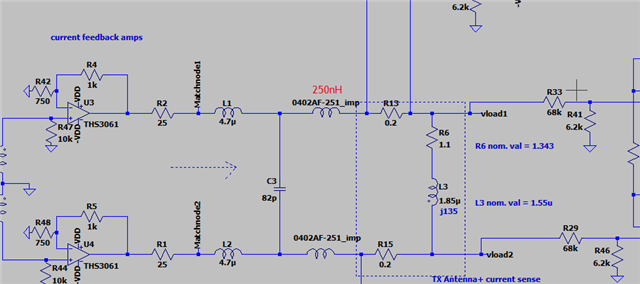
  • btw, to get to my original design, the matching network should be as below (it is an LCL, instead of a CLC).  The CLC was done later as I was changing the match to a new antenna design (R6, L3).

    L1,L2=4.7u, C3=82pf, and 250nH for the other inductors produces the desired signal levels  for R6=1.343 and L3=1.55u) in the original design which was built.

    Also, the missing Inductor  (labeled j1.21k below on the left, should be a 3.3uH inductor.