Because of the holidays, TI E2E™ design support forum responses will be delayed from Dec. 25 through Jan. 2. Thank you for your patience.

This thread has been locked.

If you have a related question, please click the "Ask a related question" button in the top right corner. The newly created question will be automatically linked to this question.

TLV07: Building instrumentation amplifier using TLV07. Why is rise time so high?

Part Number: TLV07
Other Parts Discussed in Thread: INA818, OPA320, OPA325, ADS8326

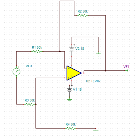
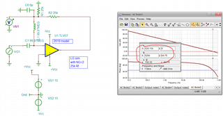
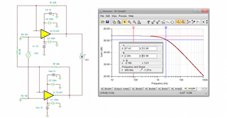
We are trying to implement instrumentation amplifier using tlv07 opamp to amplify 10mV signal 500 times. The circuit is something like this(the voltage source provides -10m step signal)
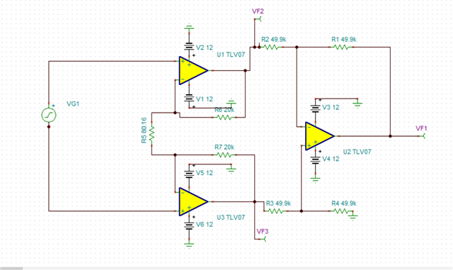
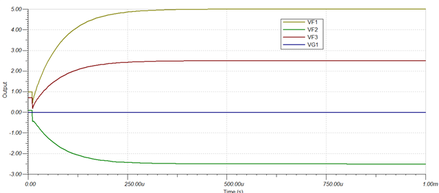
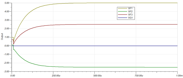
Why is the rise time so high (~0.250ms)? Is there a problem with the circuit? Or is there a problem with the op-amp, in which case request you to suggest a similar op-amp around the same price range. Also  we want to implement INA using discrete opamp for research purposes, hence we don't wish to use INA chips. Any suggestions for improvement in the circuit are greatly appreciated. Thanks Slight smile

  • Edit: I am not sure if the output is visible in the post, if not here it is:

  • well, you front end noise gain is 501, for a 1MHz GBP, that means it will have a F-3dB of 2kHz or time constant of 1/(2pi2kHz) = 80usec give a rise time for a single pole response of 2.2*80u = 175usec. Sim looks right, you need to use this calculation to set a min GBP in your solution op amp for the rise time you want. Also, I would not use such high R's in the differencing stage (lots of noise etc, although the 1st stage will dominate that) - maybe more like 4.99k values

  • Also, I would not use such high R's in the differencing stage (lots of noise etc, although the 1st stage will dominate that) - maybe more like 4.99k values

    Won't this increase power consumption though? Also thanks for the answer about GBW, makes sense!

  • Of course, but I think if you look at the numbers is is a small effect in the overall power consumption. 

  • Apart from noise is there any other major issue (related to stability etc.) in using higher resistor in differencing stage? I referred to functional diagrams in the datasheets of INA818, 826 etc. and they seem to use higher values like 40k, 50k etc which is why I also used them.

  • Hi Desiree,

    stray capacitances and chip input capacitances play a more dominant role and result in a higher degradation of balance. This might not play a role when having these resistances on the same die but with a discrete design it will.

    What is your signal bandwidth? Where is the input signal coming from?

    Kai

  • stray capacitances and chip input capacitances play a more dominant role and result in a higher degradation of balance. This might not play a role when having these resistances on the same die but with a discrete design it will.

    Thanks for this insight! So should I make the resistances as low as 5k?

    What is your signal bandwidth? Where is the input signal coming from?

    Signal is DC coming from a bridge sensor circuit.

  • Morning Desiree, 

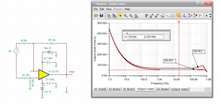
    Yes, going to 5k was perhaps too far - at 50k R's in that second stage you are at about 55deg phase margin, which is not bad and only slightly peaked in the output noise. Going to 25kohm fixed that (about 70deg phase margin) and is slightly lower output noise with no peaking. Input referring that by your high gain 1st stage makes these acceptable for noise, 

    I will say, if you care about power, the supply current range on the TLV07 is kind of remarkable - 930uA typ to 1.8mA max per channel? 

    There are other parts with tighter control I would think, 

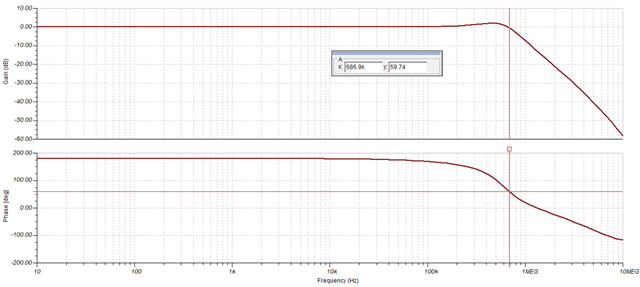
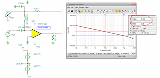
  • Thanks Michael! I have one query though, how did you obtain 55 degree phase margin? I simulated the AC transfer characteristic of the circuit with 50k ohm resistor and obtained the amplitude and phase plot as shown below. I am getting phase value of 59.74, so shouldn't phase margin be 180-(phase)? 


  • Well mapping the loop gain (LG) to closed loop is a whole different and larger topic, You are running closed loop showing about the peaking I would expect from a 55deg phase margin, 

    Here is the LG sim results, with 25kohm showing about 65deg phase margin (which will be flat closed loop response)

    Here is this file if you want to exercise it some more, 

    TLV07 diff amp LG.TSC

    And here is an article describing what I am doing here, 

    https://www.planetanalog.com/stability-issues-for-high-speed-amplifiers-introductory-background-and-improved-analysis-insight-5/

  • www.planetanalog.com/.../quote]

    Thanks for this! The article covered a lot of things I was confused about.

  • As I noted in the article, this is indeed a confusing area - and it doesn't help with all the legacy partially correct info out there - hence the article to try to clarify this relatively important, but complex, issues. Have fun, I would look for a tighter supply current spread device actually. 

  • I would look for a tighter supply current spread device actually. 

    Yes, I am looking for one. Thanks for the advice!

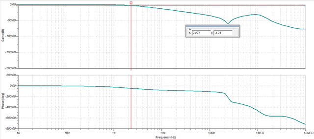
    I have another small query related to bandwidth of the instrumentation amp. I am looking at the transfer characteristics of the entire instrumentation amplifier and it is as follows:

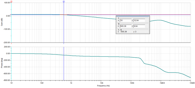
    My question is how is the bandwidth defined for a response like this? Should I still be looking at -3dB point, in which case it is 2.27kHz. My next question is, is there anyway to mathematically approximate the bandwidth of the INA from the amplifier bandwidth? I assumed it should be 1MHz/501 (noise gain of first stage). But it doesn't hold if I make the noise gain of stage 1 upto 1001, in which case the -3dB point corresponds to ~1kHz mathematically but the bode plot says around 565Hz.

  • Well yes, at higher gains the phase margin approaches 90deg and you get the far right point on figure 4 in the article, as you reduce gain and phase margin reduces you are moving left on that plot and you will ge a F-3dB BW extension - I am guessing this is not taught in the schools as I had never seen it until I derived it. 

  • I am guessing this is not taught in the schools as I had never seen it until I derived it. 

    Indeed. None of this is explored in unis. These forums and articles are holy grail :)

  • well, you front end noise gain is 501,

    Isn't noise gain for each of the individual opamp half of this (1+20k/80.16= 250). I read that noise gain of remains same regardless of configuration. In that case, shouldn't rise time be half of the obtained value then? Please let me know what I am missing here. It doesn't affect my application much but I would really like to gain a good understanding of the theory behind these things.

  • Well for the diff amp input like you have, you can split that Rg= 80ohm into two pieces and ground the middle and the differential signal will think it is seeing the same thing as what you have, Hence the noise gain is 1+20k/40ohm = 501V/V. To test, run the SSBW for the first stage where we would predict a SSBW of 1.1MHz/501 = 2.2kHz, we get 2.28kHz? The model sims as a 1.1MHz GBP. One of the themes here is when you are checking stuff like this, you need to verify what is actually in the model, not what is in the datasheet necessarily. It looks like the 1MHz in the datasheet is that slightly erroneous Aol = 0dB crossover instead of the 1pole projection to Aol=0dB that I get by looking at the Aol=40dB point then take that X100. If the noise gain was actually 1 +20k/80 this would have been a 4.39kHz - way different and not what we get. 

    yes, here is that Aol test sim where you can see the 40dB point on the Aol projects to 1.1MHz GBP (which is what you need for higher gains and many other things) while the actual Aol = 0dB crossover is at 1MHz which is what was erroneously reported as the gain bandwidth product - this is due to higher frequency poles pulling this down a bit. Not a big error here, but sometimes it is and very very very common. 

  • Incidentally, I do tend to trust the TINA model Aol curve even if they are not interpreting it correctly - one of the very key steps in model building is to get that Aol gain and phase to match full cadence designer sims so it is usually pretty reliable. 

  • Well for the diff amp input like you have, you can split that Rg= 80ohm into two pieces and ground the middle and the differential signal will think it is seeing the same thing as what you have, Hence the noise gain is 1+20k/40ohm = 501V/V.

    Thank you! This makes sense.

    The model sims as a 1.1MHz GBP. One of the themes here is when you are checking stuff like this, you need to verify what is actually in the model, not what is in the datasheet necessarily. It looks like the 1MHz in the datasheet is that slightly erroneous Aol = 0dB crossover instead of the 1pole projection to Aol=0dB that I get by looking at the Aol=40dB point then take that X100.

    This is interesting to know. I remember coming across this in your article as well.

    I would like to clarify another thing regarding the system. We are looking at the possibility of driving a low sampling ADC without any additional amplifier, hoping that the third opamp of the designed instrumentation amplifier would be able to do the job if the sampling rate is low enough and RC charge bucket filter is suitably designed. For determining the suitable sampling rate , should I be looking at the bandwidth of the entire instrumentation amplifier (~2k) or just the second stage opamp (~1MHz). I feel it should be the second stage opamp because while driving the ADC it is the one that will be supplying the current and hence only it's speed should matter in this case. This should allow me a sampling rate of ~5 ksps. Please correct me if there is any mistake in my reasoning.

  • The stage right before the ADC is what the ADC cares about for sampling settling. 

  • The stage right before the ADC is what the ADC cares about for sampling settling. 

    Thanks for the clarification!

  • Hi Desiree,

    do you plan any input filtering? Has the bridge contact to outer world?

    Kai

  • Hi Kai,

    Could you clarify what you mean by input filtering? Is it the RC filter before the ADC? I haven't explored issues related to external noise etc yet so I am not sure about this. The bridge is part of a load cell for weight measurement.

  • Hi Desiree,

    It is common for there to be an RC network in between the output of an input op amplifier and an ADC input that follows it. The right R and C selection between the op amp output and ADC input optimizes the ADC settling time as Michael infers. Since it is series resistor between the op amp output and ADC input, with a capacitance from the ADC input to ground, it has the appearance of a first-order RC low-pass filter; hence, the reference to an input filter. The net result when the best R and C values are applied helps maximize the ADC performance.

    The selection of the correct R and C values used between a particular op amp and particular ADC is not a simple matter, and is really quite involved. TI has thousands of hours developing and perfecting the techniques that can be used to determine their values, and the information is presented in the TI Precision Labs series. Here are links to the Precision Labs ADS series on the subject:

     https://training.ti.com/ti-precision-labs-adcs-introduction-sar-adc-front-end-component-selection?context=1139747-1140267-1128375-1139106-1128643

     https://training.ti.com/ti-precision-labs-adcs-selecting-and-verifying-driver-amplifier?context=1139747-1140267-1128375-1139106-1134078

     https://training.ti.com/ti-precision-labs-adcs-refine-rfilt-and-cfilt-values?context=1139747-1140267-1128375-1139106-1134075

     https://training.ti.com/ti-precision-labs-adcs-final-sar-adc-drive-simulations?context=1139747-1140267-1128375-1139106-1134076

    There is a lot of material in these sessions and it certainly takes some time to cover, but it is one of the best resources on the subject that I think you will find.

    Regards, Thomas

    Precision Amplifiers Applications Engineering

  • Thank you very much Thomas! I will certainly go through these!

  • Hi Desiree,

    Do you have all the information you need? If so, I would appreciate it if you could close this e2e inquiry. You can always open a new one if you have another question.

    Thanks, Thomas

    Precision Amplifiers Applications Engineering

  • Sure. Thank you Michael, Thomas and Kai for all your help!

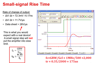
  • Just to add my two cents, for a small input signal like 10mV the rise-time of any circuit is a function of the effective bandwidth, t_rise=0.35/fc, where fc=GBW/Gcl, and not a function of slew rate.  Thus, for TLV07 with GBW of 1MHz in close-loop gain of 500, the rise-time = 0.35/fc =~175us - please see the following training material: 

    https://training.ti.com/ti-precision-labs-op-amps-slew-rate-introduction?context=1139747-1139745-14685-1138801-13228


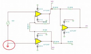
    Also, even though simulation may not show the problem, your circuit as shown below will NOT work in the real world without referencing the input common-mode voltage to the system ground (it is floating on your schematic) - without it there is no path for the input bias current flow and thus the input common-mode and output voltage would collapse on one of its rails.

  • Hi Desiree,

    assuming a 1k load cell with 1mV/V sensitivity, 0.15mV/V offset voltage and 12V maximum excitation voltage, I would probably do it this way:

    desiree_tlv07_1.TSC

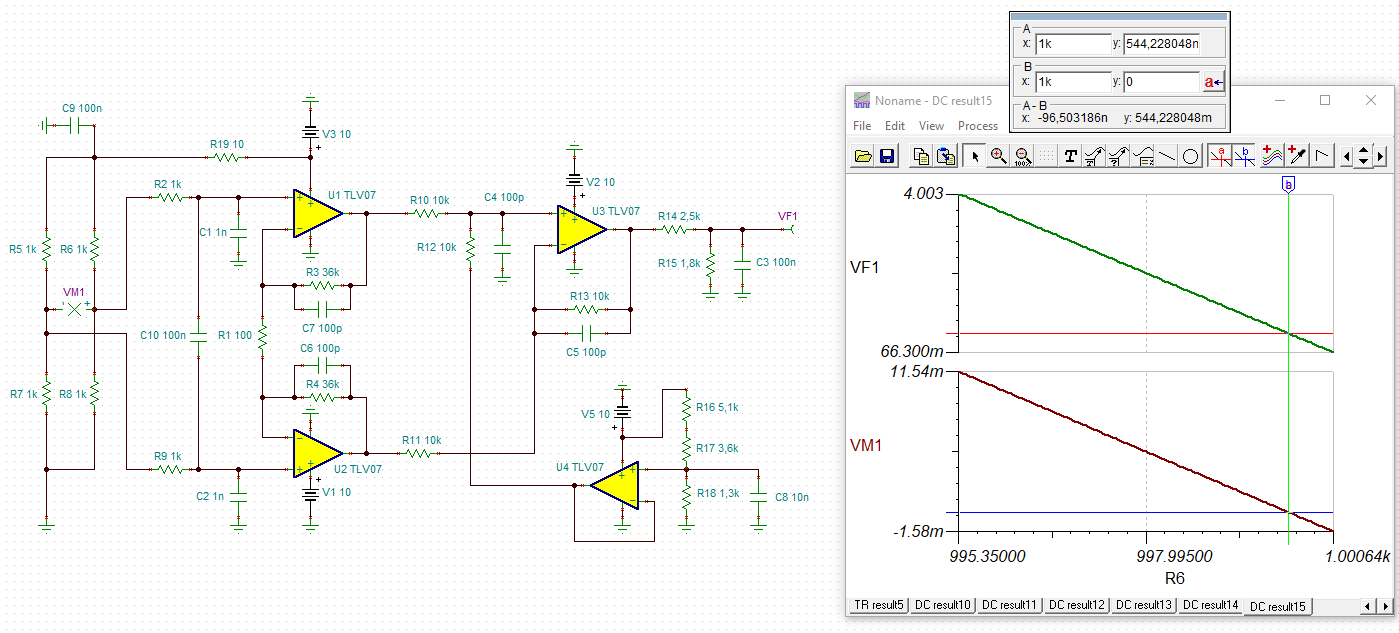
    The whole circuit uses 10V single supply. The bridge is supplied with 10V as well. To reduce unwanted and destabilizing feedback via the common supply voltage, the bridge excitation voltage is filtered by the help of R19 and C19. R19 can be increased a bit. C9 can increased by a much more extend, if needed.

    R2, R9 and C10 form a differential low pass filter. C10 can have any value between 10nF and 100nF.

    R2, C1 and R9, C2 form common mode low pass filters. C1, C2 can have any value between 100p and 1n. Keep in mind that any imbalance of these two common mode filters will degrade the common mode rejection of circuit. So take better 1% toleranced parts for R2, R9, C1 and C2.

    The output of circuit (VF1) is expected to be connected to the ADC input of ATMEGA328, a µC I work with a lot. R14 and R15 form a voltage divider to translate the output voltage range of TLV07 of 0...+10V to 0...+4.19V. The absence of negative supply voltage and the voltage divider allow the µC to be directly connected to the circuit's output without the need of protection circuitry.

    The Vref of ADC is expected to be 4.096V and 100 samples per second are expected to be drawn.

    To be able to handle the negative going offset error voltage of bridge, U4 generates an offset voltage of 1.3V. Together with the voltage divider, the input voltage range of -1.5mV...+11.5mV coming from the bridge is translated to the range of about +90mV...+3.998V with the zero input voltage coming from the bridge translated to +544mV.

    C3 together with R14 and R15 form the charge bucket filter. C3 is 100nF/14pF=7143 times bigger than the 14pF sample and hold capacitor of ADC. Because of this, during the charging of sample and hold capacitor C3 looses way less than 1LSB. Remember the ADC of ATMEGA328 is 10bit.

    The ADC wants a source resistance of less than 10k according to the datasheet of µC. R14 and R15 form a source resistance of 1/(1/2.5k + 1/1.8k)=1.05k. So this is adequate.

    About 1k source resistance and 100nF charge bucket capacitance form a time constant of 100µs. When sampling every 10ms -according to 100 samples per second- U3 has 10ms/100µs=100 time constants to recharge the charge bucket capacitance again which is more than enough.

    As you said that the signal bandwidth is DC, taking 100 samples per second should be sufficient.

    The 100p caps are for a bit of noise filtering and enhancing the phase margin. As the TLV07 is rather docile these caps are not really necessary but a nice to have Relaxed

    Kai

  • Kai,

    Nicely done!

    Thomas

    Precision Amplifiers Applications Engineering

  • Thank you, Thomas Relaxed

    Kai

  • Thank you so much. This is so helpful! I am very grateful!

  • Thanks for this insight! I will keep this in mind!

  • Hi Kai,

    I had a question related to this... I followed the precision lab videos related to ADC RC charge bucket filter design and it was mentioned that, without the use of one, a much higher bandwidth opamp is required. However, my question is, won't the low pass filtering action of the RC filter limit bandwidth anyway? My question is, for a high sampling rate, higher bandwidth opamp is desired but putting a low pass filter will restrict that bandwidth and yet it assists in faster settling. Seems contradictory to me, would really appreciate if you could clear that up.

  • Hi Desiree,

    not quite sure whether I understand you correctly.

    When it comes to driving an ADC input providing a switched sample capacitor, the settling time counts. In my example the whole charge transfer is done by the 100nF capacitor. It can fully load the sample capacitor showing an error of way less than 1LSB. The OPAmp does not contribute to this charging at all. It even does not see any change at the output due to the action of RC filter.

    But, of course, with this method only low sampling rates can be performed. A faster method is to let the OPAmp charge the sampling capacitor by its high speed and fast settling time. Then the charge bucket filter can look much less heavy and its only duty is to support the charge transfer. The charge bucket filter comes with a way smaller series resistor R then and the circuit must be designed to keep the OPAmp stable.

    Such a charge bucket filter is way more complicate to design and needs a very careful transient analysis by the help of a good simulator. It must be able to settle to <1LSB within the sampling time of ADC and the OPAmp must run stable whithout erosion of phase margin.

    In such a situation its extremely helpful, if the manufacturer of ADC already recommends a suited ADC driver Relaxed

    It's funny to see, that sometimes an ultra fast fully differential amplifier is needed to drive a fast ADC, even if the wanted signal is only of low bandwidth. But the fast ADC demands the fast ADC driver then.

    Kai

  • The higher the op amp bandwidth the lower open-loop output impedance, which means you may use a larger output cap that minimizes the output droop as S/H closes with lower Riso resistor, and still assure stability and settle the output to within 1/2 LSB within the sampling time of ADC.  Thus, with higher GBW op amp you may optimize the RC filter bandwidth to allow a shorter settling time.  If you need to push the sampling rate, our best ADC drivers are OPA320 and OPA325.

  • A faster method is to let the OPAmp charge the sampling capacitor by its high speed and fast settling time. Then the charge bucket filter can look much less heavy and its only duty is to support the charge transfer. The charge bucket filter comes with a way smaller series resistor R then and the circuit must be designed to keep the OPAmp stable.

    This is the method I am asking about which I came across in the precision lab vids. Since the charge bucket filter is essentially a low pass filter, won't it limit the opamp's overall bandwidth and it's ability to swiftly charge the sampling capacitor? 

  • Yes, charge bucket in front of ADC is effectively a low-pass filter.  However, its corner frequency may still be high enough to charge the Csh within the ecquisition time to within 1/2 LSB; thus, RC may not necessarly be the limiting factor. Therefore, depending on the required sampling rate and the resultion of ADC, the charge bucket in front of ADC may or may not be the limiting factor - achieving the maximum sampling rate for a given resolution is the main challenge in tuning the RC in front of ADC.  But in general the higher op amp bandwidth, the lower open-loop output impedance and thus lower required series output resistor to drive a given output cap in order to maintain optimal phase margin to settle the Vsh input signal as fast as possible.  Please see the following training video:

      https://training.ti.com/ti-precision-labs-adcs-introduction-sar-adc-front-end-component-selection?cu=1128375

  • Hi Desiree,

    the RC filter plays not only the role of a charge bucket filter but in many cases also the role of an anti-aliasing filter. So in many instances it's just wished that the upper bandwidth of signal is limited, in order to prevent the develop of anti-aliasing artefacts and in order to limit the noise.

    Kai

  • Hi Desiree again,

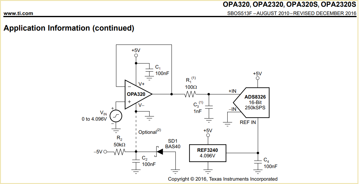
    the charge bucket filter has another advantage. To demonstrate this, see figure 44 of datasheet of OPA320, which Marek recommended:

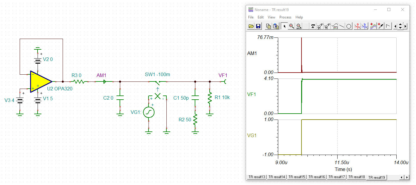
    The ADS8326 has an input circuitry which consits of a 48pF sampling capacitor in series with a 50R resistance. Without the recommended charge bucket filter of 100R and 1nF, an enourmous current spike would be demanded from the OPA320 whenever the sampling capacitor is to be charged. The OPA320 sees an effective short-circuit at the output during this period. See this huge current spike:

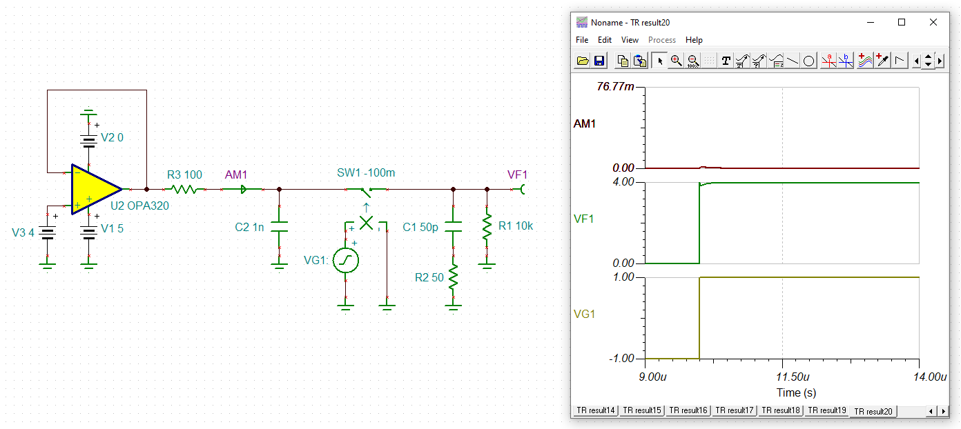
    With the recommended charge bucket filter, on the other hand, the current spike to be delivered by the OPA320 output is tremendeously reduced, because the main portion of the current spike is delivered by the 1nF charge bucket capacitance then:

    desiree_opa320.TSC

    The crucial point here is, that the loop formed by the current spike is decreased to absolute minimum, when a charge bucket capacitor is directly mounted to the input of ADC. Without this charge bucket filter, on the other hand, the loop of curent spike is extended over a considerable board space. As then considerable trace inductances can be involved, the settling time might no longer be determined by the intrinsic OPAmp's settling time but by trace inductances and other complex impedances.

    So, independently of the possible reduce of bandwidth and other presumed disadvantages of the charge bucket filter, mounting a charge bucket capacitor close to the ultra-dynamic ADC input with all its nasty switchings is just good design practice, in order to keep the board noise minimal. Omitting the charge bucket filter would do more harm than good in very most instances.

    Kai 

  • Thank you so much for this detailed insight. This is very interesting and helpful.