Other Parts Discussed in Thread: ADC3221
Hello,
I am using the ths4541 to interface to the adc3221 as described in rev C of the ADC32XXEVM schematic and very similarly, figure 80 in the datasheet. I have two configurations that are unique for each channel of the adc:
A) single ended input signal originates from a 50 ohm log amp and varies from 0.4V to 1.8V. I wish to DC couple but adjust the offset such that 0.4 -> ADC negative full scale and 1.8V -> ADC pos full scale
B) single ended input signal is bipolar centered at gnd and I wish to DC couple. scale is 1Vpp.
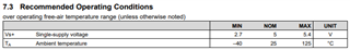
I would like to use a single power supply configuration.
1. what is the lowest supply voltage that will work in this configuration?
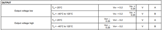
2. for B above, in particular, can the amp accept an input so far below the neg rail (0) ? I can't make sense of the datasheet; it seems the description says this is an intended application, however the common mode input low spec indicates 0.1 below the negative rail. if the input common mode voltage is Vicm = (V1 + V2)/2 and V2 = 0 and V1 = sin(wt) then it will violate this spec?
3. won't the bav99 diode prevent option B ? it will turn on during the negative cycles of my input?
4. still connect the ADC VCM of 0.95 to amplifier Vocm, correct?
5. for input A above, can the offset correction be handled by tying R1 and R5 (fig 80) to (1.8 - 0.4) = 0.7V ? will that add HD as neg input would be AC only coupled to gnd while the pos input is DC coupled?