This thread has been locked.

If you have a related question, please click the "Ask a related question" button in the top right corner. The newly created question will be automatically linked to this question.

INA128 Bandwidth

Other Parts Discussed in Thread: INA128, INA217, INA163, PGA202, PGA206

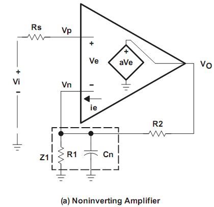
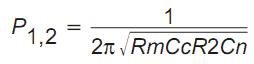
Working with INA128, single supply, ac coupled, driving high pass, single-pole RC filter with impedancee around 17 kohms. I see that the gain vs frequency has shifted away from the typical performance characteristics, and the 40dB gain roll-off is now around 20 kHz vs specified value of 80-90 kHz. What could cause this to change?

  • Hello Dennis,

    Sorry for the delay on this…I was on vacation until yesterday.

    I have attached a TINA schematic that I believe represents your circuit.  Can you please modify it as requested in the schematic?  If you don’t have TI-TINA, it can be downloaded for free here:

    http://focus.ti.com/docs/toolsw/folders/print/tina-ti.html

    On a sidenote, I do not believe that you can modify the equations in the schematic with the ‘free’ version of the software.

    dennis.TSC
  • Hi Pete,

    I have attached the .jpeg of the schematic of the circuit I am working with.  Analysis won't run because of irregular (???) circuit.  Circuit seems to work well when there is no analog switch involved, and  I can't seem to get around that problem.  I did not try analysys without capacitance of the analog switch because I am happy with circuit performance in that configuration.  I get a very limited bandwidth when the switch is connected -  starts rolling off at about 20 kHz.!!

     I tried to insert the TINAS schematic file but I got a notice that it was an invalid file (???) when I tried to insert the file.  I was looking for an attachment feature but dont see it..

    Thanks much for your counsel, Pete.

  • Hello Dennis,

    Thanks for the additional details.

    I have attached an updated TINA schematic...please take a look.  I believe your 'irregular circuit' issue is due to your voltage source not being grounded.  Also, in order to attach a file you have to select the "Options" link toward the top of the page.  One more thing...I notice your Vref is 5V.  With 50mVp and a gain of 100, the output will clip.  I adjusted the Vref to 9V.

    The simulation does not show a 20kHz BW limitation.  Let me continue thinking about the issue and get back with you.


    fromdennis.TSC
  • Hello Dennis,

    Upon further investigation, I have a few additional questions and an observation.

    First, please note that the capacitance on the gain-setting pins (inverting terminals of the amplifiers) due to the analog MUX/switch can lead to instability due to the topology (non-inverting amplifiers) as discussed in the attached application note.

    Questions:

    a) Are the capacitors truly imbalanced (100pF and 200pF)?

    b) Are those values accurate? They seem rather large.

    c) How are you measuring the bandwidth?   

    d) Do you see the output oscillate given a step input?

    My TINA simulations do not seem to be re-creating what you're experiencing on the bench, so we need to rely on your data.


    sloa013a.pdf
  • Hi Pete,

    a) Using Analog Devices, ADG1402, 4:1 Mux.  The typical capacitances are: 150pF at common terminal and 39pF at switch terminals in OFF state.  In the ON state they are 217pF at all terminals.

    b) I picked some arbitrary values for the TINA schematic setup, but they were in the ball park for some of the gains settings.

    c)  I confused the issue when I mentioned bandwidth in a pure form!  Here's the problem:  With the capacitance at the switch terminals, the output of the INA128 starts to peak around 20kHz.  The peaking increases with decreasing gain.  Couple this phenomena with the natural roll-off of the INA128, which decreases with higher gains, and the result is changing bandwidth with gain.  From a system view point, that would cause a significant calibration problem.  I have a 1000 channels and 5 different gain settings on the first stage gain and 16 settings on the second stage gain.  Ideally I can come up with a circuit design that would give me the same bandwidth at all gains.

    d) I took your last TINA schematic and analyzed it with no capacitance at the terminals of the switch, and the response was flat as expected.  Then I replaced the switch with an Intersil part with lower capacitance, but higher on-resistance. I used a 10pF  and  5pF capicitors.  The amount of peaking decreased significantly at 0dB gain.  Then I added a low pass filter at the output of the INA128 (1000 ohms and 1.5 nanofarads) in order to control the bandwidth (106kHz).  Analyzing these circuit changes almost yielded the desired results, but the 40dB gain setting is rolled-off a little too much.  I am not sure that the filter is the right answer, and the increased MUX switch on-resistance is also a problem at the higher gain settings.  I am looking for any comments and/or suggestions for a better solution.  I like the INA128 because of the operating voltage range and the noise floor.  The specification suggests that I should be able to get a bandwidth of 70kHz out of the part - my target.  The peaking restricts the target bandwidth given that I need a constant bandwidth over varying gain.  I have not analyzed with a step input yet - I have TINA on my home computer because of a firewall problem at the work site.  I will try the step input tonight.

    I sure do thank our for your help with this design.  Your counsel speaks well of your engineering skills and your company's commitment to the customers.

    later<><><>


  • Hello Dennis, Thanks for the additional information. I am travelling today, so I will have limited access to e-mail. I will do my best to get back with you tomorrow.
  • Hello Dennis,


    Thanks for your patience.  Here is a discussion of the capacitance on the inverting terminal of a non-inverting amplifier.  I am focusing on the input.


    Gain-peaking will occur due to capacitance on the inverting terminal.  Given the following general diagram of a non-inverting amplifier:


    We expect to see a zero at the following frequency:


     Where: 

    R1=gain-setting resistor (1/2 Rg for the INA128)

    R2=feedback resistor=25k (internal to the INA128)

    Cn=capacitance at non-inverting terminal to ground


    The capacitance will also create a complex conjugate pole at: 


    Please notice that the frequencies of the zero and poles are inversely proportional to the capacitance.  So, as the capacitance goes down, you should see the peaking later in frequency. 

    The gain of the INA128 is inversely proportional to the gain-setting resistor and the gain-setting resistor (R1) is inversely proportional to the frequency of the zero (it does not play a part in the frequency of the poles).  Therefore, there should be a direct relationship between the start of the peaking (the zero) and the gain of the device. 

    The frequency of the poles, however, will be determined by R2 (25k) and Cn.  We do not have access to R2.  It should be noted that Rm and Cc are parameters that deal with the device’s design and are essentially fixed.


    Please note that the Ron of your switch will be in series with the gain-setting resistor (R1).  I assume that it is small in comparison to R1.


    After re-reading your e-mail, I believe all of this theory is consistent with your observations.  Correct?


    Based on the theory above, we need to decrease R2, decrease Cn, or both.  R1 values will be dictated by the required gains and the selected device's gain equation.  Therefore I would recommend looking for a switch/MUX that has the lowest capacitance and Ron as possible. 


    Concerning the INA128, you stated that you like the operating voltage (4.5-36V) and noise.  Your gain needs to be adjustable and varies from 1 (0dB) to 100 (40dB).  Out of curiosity, how many gains (and values) are you switching between?


    A couple devices that you may want to investigate are the INA163 and INA217 (have smaller R2 values but supply is 9-36V).  The INA163 also provides access to the outputs of the input-stage amplifiers which would allow you to perform some compensation as described in the aforementioned application note, but comes in a 14-pin package.  The noise figures are in the attached PPT file.


    I hope this helps. 


    noise comparison.ppt
  • Hello Dennis,

    I made a mistake...

    Cn=capacitance at the inverting terminal to ground

    Sorry for any confusion.

  • Hi Pete,

    Very interesting and detailed analysis.  I caught the inverting terminal, and I was confused about the complex conjugate pole. 

    However, from direct measurements of the circuit, I see two poles: one at approximately 2 Hz and the other around 20 kHz.  Would the first pole be fz and the second, P1,2?  I did not analyze the TINA circuit in a way that I could see the very low frequency pole, but I will try that next.  Are there some typical values for Rm and Cc?

    I also analyzed the circuit with a step input.  There was no ringing at all, but an interesting phenomena!!  At 5 ms there was a negatively going glitch that varied in width with the capacitance.  It was present with all gains.  The 5 ms time was constant (???).  Any ideas on that one.  I don't see that in  the actual circuit, not yet at least!

    I looked at the INA163 and INA217.  The noise is excellent, but the package is maybe a problem!  That has to do with the notion of making this whole circuit very small.  The intent is to make this signal conditioning circuit an inline circuit such that it is about the size of a big cigar!  This is being done to defeat an extremely high magnetic EMI environment.  Anyway, I will continue to look into the INA  amplifier options.  The lower value of R2 in your suggested parts is also a significant consideration.

    Your counsel have been most helpful in solving the design problems, and I thank you.  The development horizon is much clearer now!!! 

    The TINA introduction has been beneficial as well.  By the way, do you know of any documentation out there that covers the details about the application of the TINA  setup and analysis?

    Oh, I forgot  --  I am switching five (5) gain settings  -- 0 to 40dB in 20 db steps. 

    Thanks again, Pete.


  • 8831.Getting Started with TINA-TI.pdf

    Hi Dennis,

    I can direct you to some TINA documentation. I attached TI's TINA Quick Start Guide which is off of our website.

    Another useful resource is the DesignSoft TINA website. You can find more TINA documentation and video tutorials.

    Best Regards,
    Chris

  • Hello Dennis,

    Thanks for the additional information concerning the various gains you're using.  I'm assuming you mean 0dB to 40dB in 20V/V increments.  That would correspond to 1V/V, 20V/V, 40V/V, 60V/V, 80V/V, and 100V/V.  I was hoping to find a PGA or combination of PGAs that would work for you (e.g. PGA206/7 or PGA202/3), but the 60V/V gain can't be realized by either combination and the 100V/V can't be realized by the PGA206/7 combination. 

    The pole that you're seeing at 2Hz is probably due to your high-pass filter.  I do not have the typical values for Rm and Cc for the INA128.

    I understand that the packages of the INA163 and INA217 could be an issue.  But, I recommend prototyping them to see if they have an effect. 


  • Hi Pete,

    The steps between a gain of 1v/v and 100 v/v is really 10dB, so there are only 4 steps.  That does not provide for a PGA option very well.  I am prototyping the circuit with a different analog switch with less capacitance, and according to the TINA analysis that should give me control of the bandwidth where I want it.  I looked at the 163 and 217 with a lower R2 value, but the package size and lower resistance caused problem when compared to the analog switch "on" resistance.  I am also looking at digital pots, but they have some capacitance too. 

    So, bottom line, I hope this prototype pans out!!

    The 2 Hz phenomena is still a mystery.  The analysis indicates that the high pass filter at the input should be at about 9Hz, and it is a nice 6dB/octave roll-up like I expect.  The phenomena shows up on the signal analyzer measurement as a "hook" in that well-behaved 6dB slope!!  It is only seen when the gain is 1 or Rg is open (as much of an open as the analog switch can provide when it is disabled).  I can't seen any other components that can produce any poles or zeros around that frequency.  Could there be a cross-over mismatch in the poles at the differential inputs causing a "glitch" in the HPF response?

    Alas!!

    Later<><><>