This thread has been locked.

If you have a related question, please click the "Ask a related question" button in the top right corner. The newly created question will be automatically linked to this question.

THS4521: How to design a shematic with an amplifier to support more than five inputs?

Part Number: THS4521
Other Parts Discussed in Thread: LMH6702, OPA695, OPA855

Hello:

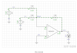
I want to design an adder with an amplifier to support more than five inputs.

Just refer to the example as below.

Besides, the frequency of the inputs is almost 200Mhz.

Would you please suggest me an amplifier and a referrence schematic?

Thanks a lot.

  • You will likely need to use a current feedback summer to get the BW. A part like the OPA695 or LMH6702 might work. You will have to use lower R values, around 402 ohm each if you want unity gain on each channel, yes, this looks pretty good using 402 for all R's

    5 channel inverting summer OPA695.TSC

  • So lets say we wanted to to the same thing with a VFA, 5 gain of 1 inverting channels will give you a noise gain of 6, say you wanted about 400Mhz F-3dB to keep each channel flat through 200Mhz, that then is 2.4GHz Gain bandwidth product. Yes, there are parts like that, perhaps the OPA855

  • Thanks a lot.

    The file attached just shows the example, all right?

    I can not open this file with extention of TSC.

    Would you please upload a screenshot of this example?

    Thanks a lot.

  • So that prior file was V9, here is a V7 version 

    8255.5 channel inverting summer OPA695.TSC

  • Woudl you please give me an example of designing a transimpedance amplifier with OPA855?

    It can be used as a transimpedance amplifier, which is described in the datasheet.

    Thanks a lot.

  • Hello,

      We would need more details, then we can assist in building a simulation file with the OPA855. 

            1) input source (photodiode) capacitance

            2) input current range 

            3) rise time of the pulse

            4) Gain 

            5) load, second stage interface?

    Thanks,

    Sima 

  • What simply works at low frequencies need not necessarily to work at high frequencies. Already mounting five or even more feedback resistors to the -input of HF OPAmp alone, might introduce so much wiring inductance and stray capacitance that the OPAmp might begin to oscillate.

    Because of this, you need to decrease the number of channels which shall be summed by one single OPAmp. And to reach the number of channels you want to sum, cascade these summing amplifiers.

    Keep also in mind, that the input summing resistors must be driven by a low source impedance, sufficiently low up to the highest frequencies. Otherwise the summing amplifier can become unstable. Therefore, it would be a good idea to drive the input summing resistors by individual OPAmp buffers.

    Then, as it is difficult (or impossible) to match the impedance of microstrip line to the impedance of input summing resistor, keep the wiring length to the input summing resistors to the absolute minimum. A 51R isolation resistor directly at the output of driving OPAmp can be helpful.

    The following schematic shows how I would do it:

    user_opa855_2.TSC

    Of course, this is only the first stage of cascading. Further cascading stages are necessary, if you want to sum more than five input signals.

    And, please remember, what I said above: If the unavoidable routing inductance and stray capacitance of five input channels already results in instability, you might need to decrease the number of input channels.

    Kai

  • G8931-04 is used as the photodiode in this design, which is released by HAMAMATSU.

  • Thanks a lot.

    How about the VCC of OPA855?

    Are you using a split supply or a single one?


  • Your last post is kind of confusing. First you say you want to build a summing amplifier. Then you say you want to build a TIA...

    Kai

  • Well yes Kai, the questions seem disconnected and poorly defined. If we are veering off into a transimpedance design, perhaps should start a new thread to isolate the issues. And, Sima listed what would be needed to go further with transimpedance, no reply on those essential points yet? not really possible to proceed with this lack of detail. 

  • Hello,

       As Michael and Kai have already suggested, it would be better if we moved the TIA design to a new thread. I will close this thread, please make a new thread with OPA855 part number and information to these questions:

            1) input source (photodiode) capacitance

            2) input current range 

            3) rise time of the pulse

            4) Gain 

            5) load, second stage interface?

    Thank you,

    Sima

  • In fact, it's not confusing. I want to make use of five APD.

    I'm going to build a TIA for each APD and make an adder to support the outputs of these TIAs.

  • Hello,

       From the above, these five APD will be G8931-04, is this correct? In that case, the capacitance of each diode will be 0.35pF at the highest bias reverse voltage. Check the figure in the APD datasheet for capacitance if using a lower reverse voltage.

       Looks like also the range is between 1nA to 100uA. But again, this is dependent on your wavelength and reverse voltage. If we have this information, we can narrow it down to a certain range, and from there we can narrow the gain which is also dependent on your desired output voltage. 

       For rise time, looks like this is a pretty fast APD with about a min 88ps. This will be difficult to achieve, we would need confirmation on what range you are looking for here.

    Thank you,
    Sima

  • The reverse voltage is about 54V and the wavelength is about 1550nm.

  • Hello,

      Thank you for the information. I forgot to mention that I would also need the amount of power to determine the current using power, wavelength, and photosensitivity (found in datasheet). 

      For now, I have it as max current at 100uA, and I have the gain set to 10kOhms which will give you a closed loop bandwidth of around 603MHz for a Butterworth response using the OPA855, which is our 8GHz decompensated amplifier. This would follow the setup Kai proposed above. For a very high speed part like the OPA855, wiring inductance and stray capacitance will be critical or the amplifier will oscillate. 


       We can help create a simulation using the OPA855. This will work for pulses with min rise times of around 580ps. Will this work for your type of application?

    Thank you,

    Sima 

  • Well Sima, if he is looking for a summing BW of 200Mhz, probably do not need that 600MHz in the Zt stage. Also, that Cf solution for 0.04pF might be a challenge, we used to use PRP resistors for sub 0.05pF parasitic. (Precision Resistive Products, red buf axial R's - they were common in network analyzers)

  • Hello Michael and user,

      That is correct, the feedback capacitance calculated would be very difficult to realize in practice. Thanks for the additional knowledge on PRP resistors! I was not aware of these.

      Also for noting the correction on the bandwidth. I was going by the APD given, but I now see that the application would need down to 200MHz. This makes this easier, here is the updated calculation while still assuming the same input current and output voltage requirements as stated earlier:


      Would only now need a sub 1GHz GBW part. These products should work for this type of application. Can be filtered down on noise/dc/power/supply requirements. 

    Thank you,

    Sima