This thread has been locked.

If you have a related question, please click the "Ask a related question" button in the top right corner. The newly created question will be automatically linked to this question.

THS3061: Determining Feedback Resistor Values for Gain Values

Part Number: THS3061
Other Parts Discussed in Thread: THS3062, , OPA695

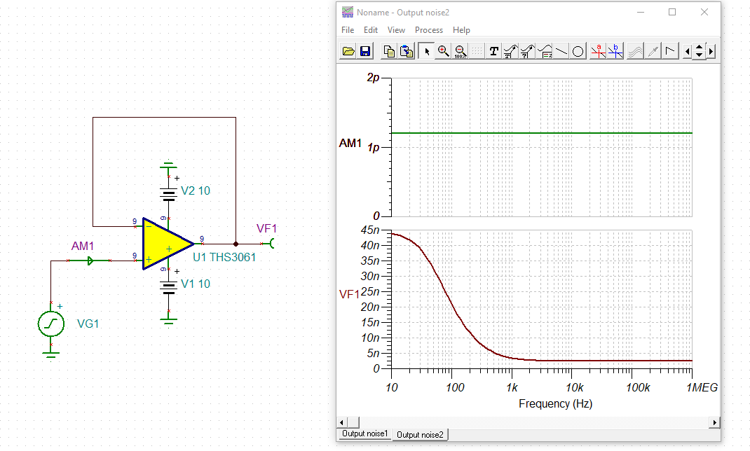
I'm looking at using the THS3061 op-amp (and by extension, possibly the THS3062 op-amp) as part of a simple circuit to add and subtract voltages. These voltages are small-signal voltages (with amplitudes of 100 mV or lower and a bandwidth of 200 MHz). I wanted to use the THS3061 op-amp because of its high bandwidth as well as how current-feedback amplifier feedback is dependent on the feedback resistor. I figured that as a current-feedback amplifier, the wide bandwidth range will be beneficial in my application, not to mention how it isn't determined by the gain-bandwidth product as with a voltage-feedback op-amp. 

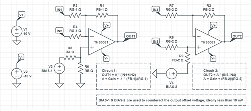
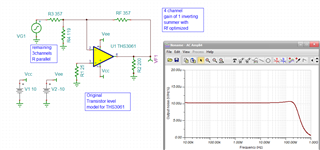
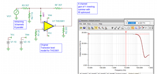
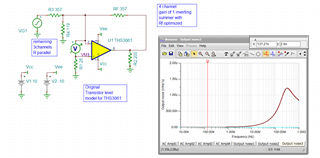
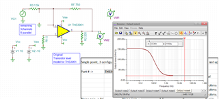
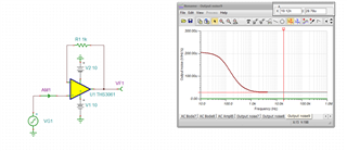
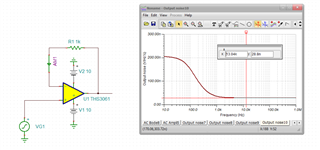
Below is an image showing how I plan to use the THS3061, adding voltages on the left circuit and subtracting voltages on the right circuit. It's a pretty simple circuit, and this is just a simplified application to make things easy to understand, but my question is with the feedback resistor values. According to the datasheet, it lists recommended feedback resistor values. Now, my application requires the gain to be between -2 and 2 for simplicity's sake. The gain may vary between these values, but through simulations, it shouldn't exceed an absolute gain of 2 for each op-amp circuit (so, one op-amp may have a gain of -2 whereas another may have a gain of 1.75). With that limitation, the recommended feedback/gain value section in the datasheets mentions that the bandwidth is inversely proportional to the feedback resistor. As gain increases, it appears that the feedback resistor is reduced accordingly. In order to keep a high bandwidth given my gain requirement, is it best to keep FB-1 and FB-2 to a fixed value (closest value I see here is 560) and adjust the RG-1/RG-2 resistor values to achieve the gains I need? 

If it helps, the op-amp circuits will be cascaded together, though it doesn't show in this simplified example. For example, OUT1 may go into the second circuit as IN3. Circuit 1 may have a gain of -2 while circuit 2 may have a gain of -2. This is just a rough example, but I hope it gets the point across.

Circuit Application

  • Hi Jason,

    it's a good idea to analyze the noise gain of your circuits and to select the resistor values accordingly.

    Kai

  • Dear Kai,

    Thank you for your reply. If I may ask for your assistance, how do I apply the input noise density model as shown in the datasheet to my model circuits? Comparing their model with my circuits, some components can seem to be roughly equivalent with each other (such as accounting for all input resistors in parallel with the feedback resistor in place of Rg), but I'm a bit lost on how to incorporate other parameters, such as the Rs term given my circuit layout. The 4kTRs as shown in the equation appears to be the Thermal voltage noise associated with each resistor (in this case, Rs, given the S superscript). Is that just a simple matter of using the resistor value, the Boltzmann's Constant, and the Temperature in Kelvin? In some ways, the formula looks straightforward, but I just want to make sure. 

  • You are on the right track, but if you really want 200MHz with multiple sources, you might look at the OPA695 instead - +/-5V supply but much faster to begin with. Do you have a minimum input R you can drive -would 100ohm be ok, 

    Kai's comment on noise gain applies 2nd order here being CFA, the feedback transimpedance is the Rf + Ri*NG where Ri is the inverting input R

    I think I put that discussion in the back of the OPA695 datasheet. 

  • Thanks for your reply. Unfortunately, due to my project limitations, the OPA695 can't be used at this time. In my worst-case design scenario, the power supply needs to be +10/-10 or more to handle the voltages. Limiting the op-amp to +5/-5 volts would most likely lead to saturation as the output reaches VCC/VEE. I don't have a minimum input resistor requirement, as long as it's not too low that it would cause unwanted distortion.

    I'm not sure if I'm doing this right, but let me show you roughly what I'm trying to accomplish. Below is a simplified schematic of what I'm hoping to achieve. I ran a rough SPICE simulation using these resistor values to get the outputs that I want from the op-amps on the far right. Using these resistor values. This results in an (absolute) gain ranging from 1.4 to 2 at each op-amp. Hence, that's why they all have the same feedback resistor as per the datasheet. Looking at each op-amp separately for noise calculations, following the formula and using the equivalent resistance at each input node (I did this by shorting the inputs going into each resistor to ground and taking the equivalent resistance), I somehow ended up with a maximum input noise density of 9.16 nV/sqrt(Hz). For the equivalent output noise, the maximum value that I ended up with is 17 nV/sqrt(Hz). These values came from the difference op-amps shown in my circuit. 

    Interestingly enough, when I ran a noise simulation in LTspice with these values, I saw that for the outputs, I had a high noise density that dropped as the frequency got higher. My method of testing may not be perfect, as I am new to noise analysis, but I saw a noise density of 255 uV/sqrt(Hz) at low frequencies coming from OA5 at the top right, which dropped down to 36 uV/sqrt(Hz). Considering how my hand calculations had it to be in the nano-volt range, this makes me curious. As gain increases with the CFA, the feedback resistor value decreases. If lower resistor values reduce the overall noise density, why not just go with the lowest recommended resistor value (in this case, 200 ohms) and work with lower gain yields?

    Simple Schematic

  • Morning Jason, 

    So the inverting summing design for CFA includes a Zopt calculation - that is trying to scale the R's to solve to the nominally correct feedback transimpedance to hit a butterworth closed loop response - the THS3061 specifies an open loop inverting input Ri of 71ohms, using that in this table of bandwidth vs gain with Rf adjusted calculates out very closely to about 700ohm Zopt. This is looking at Rf + Ri*NG (noise gain)


    You are in luck, my TINA V11 has a library model for the THS3061 - looks like an original transistor level with very thorough Q models - should be  pretty good, 

    Here is an example, 4 channel design gain of 1on each as an example - yes, optimizing to the Rf = 357ohm from the datasheet table for gain of 5 gives a very nice SSBW with about 316Mhz F-3dB and pretty flat through 200MHz. 

    The general development for this Zopt is in this original app note I wrote from from the comlinear days, ignore the obsolete statement, that is just saying none of the parts in here are available anymore, but the analysis is correct and useful. 

    https://www.ti.com/lit/an/snoa366b/snoa366b.pdf

    Here is this TINA file, V9

    THS3061 inverting summing.TSC

  • Or, just running the output noise with the TINA model gives this - once again, I would be guessing the internal noise model is just a bit off - this is surprisingly bad, or perhaps I am making some mistake - 

    here is an inverting current noise sim, looks about righ - 

    Here is an input voltage noise sim, not sure about this

  • Hi Michael,

    the voltage noise of THS3061 seems to be modelled adequately. But the current noise seems to be a flat 1.2pA/SQRT(Hz).

    Kai

  • Here is a simple gain of 1.5X output noise sim, not sure what is going on, but this noise model seems way off, Don't think we can use the TINA THS3061 model for noise sims. 

  • If I may, from my tests, it appears that as the feedback resistor increases, the noise parameter increases, yet it rolls off at higher frequencies. As the feedback resistor decreases, the noise parameter decreases as well, but at a certain high-frequency point, the noise spikes before rolling off. I've posted a simple example using TI's SPICE model in LTspice. This is a simple noise modeling circuit as you adjust the feedback resistor from 100-800 ohms to illustrate my point (green is 100 ohms, blue is 200 ohms, etc.), with the other resistors being matched for an inverting 2x gain. I have to say that it's disheartening to see that I'm getting a noise density in the micro-volt range, rather than nano-volts as I was expecting. Perhaps it's the circuit.

    Now, as the designer, I can design it any way I want. If I want to limit it to a certain bandwidth, should I be concerned with those large spikes? Seeing as how they occur at high frequencies at 400 MHz, and my bandwidth is 200 MHz, since I'm nowhere near that spike, a 100-ohm feedback resistor should be okay? Even with the roll-off at a higher value resistor as you can see, the magnitude of noise at that roll-off is less than what it would be at a lower feedback resistor at the same frequency. It feels like that spike is occurring due to a pole somehow, but does that cause instability at that frequency only?

  • Well everything you say makes sense

    1. Increasing Rf increases the gain for the inverting current noise and bandlimits

    2. Decreasing Rf decreases the gain for the inverting current noise and undercompensates leading to peaking

    3. As I showed previously, the THS3061 model is way high on voltage noise, cannot use it for noise sims per se. that is a modeling error, the part is much lower itself. 

  • Well Kai, that noise sim is not using any feedback R - looks nice but not possibly with a CFA. Not sure why it looks so nice here and if I add a 1kohm it goes to pieces. 

  • So...if the model is worthless, perhaps its better to just stick with the datasheet recommended values, but the recommended values went as low as 200 ohms. Though the magnitude may be off, does peaking still occur at the same locations?

    Speaking of which, since micro-volts is way too high, what do you expect a circuit like this to be in the range of: nano-volts? Op-amp is in nano-volts but does it depend on the circuit? 

  • Hi Jason,

    have you noticed my first noise simulation above?

    Kai

  • So the AC SSBW sims seem to work fine, I gave you an example 5 channel gain of 1 solution for optimum Butterworth, if you have a specific design point (multiple inputs, what are there gains) i can run another one. Once you have a design, the total output noise is simple to solve - using this equation, 

  • So Kai, not sure which one you are talking about but way above you seem to show a noiseless ideal op amp with noise models added externally - yes, that is a good way to execute the output noise calculation but it does not give you the right AC response for the noise terms, 

    or, your THS3061 noise sim with no feedback R looks pretty reasonable for noise, but you cannot physically operate a current feedback amp without a feedback R - once you add that, the output noise explodes up? 

    If the THS3061 model must be used, use it only for AC design responses, then use the output noise equation to estimate the output spot noise. Or use your ideal op amp with external noise to get that, but do not pay much attention to the response shape at higher F. 

  • And, going more into the noise model issue with the THS3061, here I tried to just report the inverting current noise - should be in the pA region but shows nV? probably a labelling error, but the current noise on the inverting input is apparently in the nA region, that explains the high sim output noise with a non-zero Rf it seems. Physically, it is a pretty good part, but the sim model needs some polishing it would seem.