This thread has been locked.

If you have a related question, please click the "Ask a related question" button in the top right corner. The newly created question will be automatically linked to this question.

THS3491: Use as post DAC amplifier

Part Number: THS3491
Other Parts Discussed in Thread: DAC3151, , THS3217, THS3215, THS3091

Hi all,

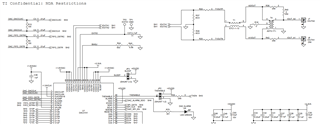
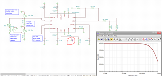
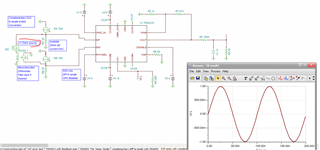
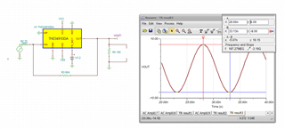
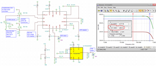
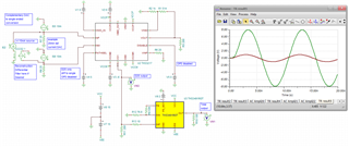
I am intending using the DAC3151 followed by THS3491 in an application that requires driving a +/- 8V into 100 ohm load at over 100 MHz.

Noise and distortion are not super critical.

What would be the recommended way to interface these two devices?

Using transformer? Using both or single current output from DAC? THS3491 as TIA or just use in normal V/V non-inverting configuration?

Any ideas or tips appreciated.

Thanks

  • Morning David, good questions, 

    I worked up the product roadmap some years back for TI here, Your swing is too high to use the THS3217 that I would be using here otherwise, 

    1. If you can be AC coupled, yes a balun into the correct termination for the DAC into the V+ input is probably the most flexible approach - just set the THS3491 gain to what you need for that input swing and adjust the Rf for flat performance. 

    2. We sometimes do a differential transimpedance here, but that gives a diff out usually using FDA's

    3. The standard diff to single stage can work, but has some balance issues and design issues with a CFA - if you do not need DC couples, I would not go this way, 

  • Hi Michael,

    Thanks for fast response,

    I do need DC coupling since this is sort of an AWG with possible DC component.

    Could you please expand a bit on your recommended solution given this new info.

    Sorry for not stating this restriction in the beginning.

    David

  • The simplest, but not the cheapest, would be to use a THS3215 or THS3217 out of the DAC and then into the THS3491. The Complementary to single ended single stage op amp requirement has an active impedance issue at the differencing amp - that is why the resistors on the two sides of the D2S stage in the those parts are not of identical value - identical ratio but the scaled to show matched impedances including the active impedance aspect of the app. This slightly improved the HD2 out of the D2S stage. 100MHz is not easy for even modest HD, look at the plots in the THS3215 and THS3217 for the D2S stage - at about -30dB THD, you can see it on a scope. 

    To do the design with a single THS3491 is a lot more work if you want to try and balance the impedances to the DAC outputs. 

    I tried this many years ago and later discovered I messed up the equations in this app note, but this will explain the issues. 

    https://www.ti.com/lit/an/sbaa135a/sbaa135a.pdf

  • Just to look a little further, I went into the datasheets for HD at 100Mhz 

    yes, the THS3215 D2S stage by itself (you can disable the OPS if you are going straight from that output to the THS3491) shows this. So at 2Vpp (requiring gain of 8 in the THS3491) it is about -50/-44dBc (HD2/HD3) into a 100ohm load - lightening that load would help. Then that HD gets degraded by the THS3491. 

    using more power in the THS3217 certainly improves this, looks to be about -54/-55dBc. 

  • So I was going to go a little further with a THS3491 only design, wow is hard to find any output interface data on that DAC - not in the datasheet as far as I can see, in the EVM schematic I see this (and of course this is not TI confidential, need to clean that out, I am guessing 50ohm equipment off board, so the DAC wants to see 25ohm on each output pin apparently -that is normal. 

  • I started looking for some prior work, here is a THS3215 D2S only sim with 20mA tail current DAC, nice and flat through 100Mhz, 

    And then running a full scale sinusoid, 10MHz, looks good with 2Vpp output to work with for the THS3491 if you want to consider this, 

    I was just looking for the source model, now on to a THS3491 single stage which I think will need a simultanous solution for the non-inverting attenuation side and inverting load. 

  • And then down the road, if I supply the THS3491 with a 2Vpp inverting I get 16Vpp and it is nice and flat through 200MHz, here is an example +/-8V into 100ohm 100MHz, next I need to set up an added R to ground on the inverting side, compute the noise gain, decide what attenuation I need on the non-inverting side, fold that signal into the active impedance that Rg becomes then set up a simultanous solution for that R to ground on the inverting side and the attenation to get a match gain magnitude on the non-inverting side. Might take awhile, 

    And here is this sim file TINA V9 - this might be an earlier version of this DDA model, but useable. 

    Inverting THS3491 sim DDA model.TSC

  • Thanks - I really appreciated your ideas.

    Will implement solution with THS3217 followed by THS3491

  • Morning David, That should give you what you need, here I combined the THS3217 using only the D2S output to a non-inverting gain stage with the latest THS3491RGT model which is a little faster package version - the DDA was done mainly to provide upgrade path to the THS3091 designs.About 620Mhz F-3dB, 


    And here is your +/-8V 100MHz output.

    Notes

    1. Keep the parasitic C on the D2S output very low, 

    2. I added a series 10ohm into the V+ input of the THS3491, helps very high F stability

    3. I used a 200ohm D2S load to keep its response flat

    4. Somewhere in here, most folks add a reconstruction filter to smooth the DAC steps. 

    5. Not using the OPS here as the THS3491 has plenty of performance and is lower HD at these conditions. 

    and this last file, 

    THS3217 D2S tests with THS3491 gain stage.TSC