Other Parts Discussed in Thread: INA321, TINA-TI
Hi,
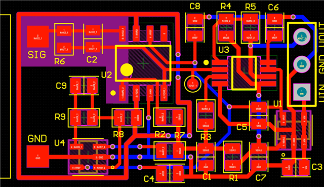
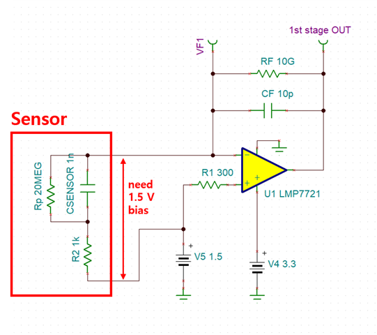
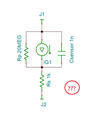
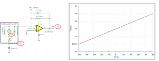
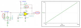
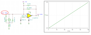
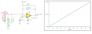
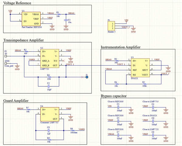
I made a two-stage trans-impedance amplifier using a LMP7721.
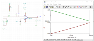
The schematic is below.
which is same to

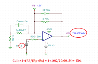
The operating point of negative input node of LMP7721 was 1.5 V.
However, when I actually made the circuit, 0.8 V was measured at the node.
The same 0.8 V was measured when nothing was connected to the node and when a capacitor was connected between the node and the ground.
How can I solve this problem?