This thread has been locked.

If you have a related question, please click the "Ask a related question" button in the top right corner. The newly created question will be automatically linked to this question.

XTR111: Level shift of 0V input and Transconductance trim

Part Number: XTR111

Hi, support team

My customer has the questions as follow:

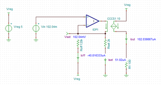
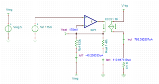
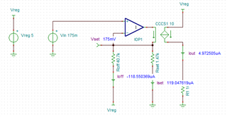
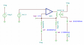
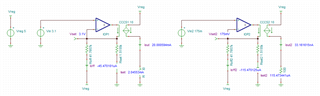
In the datasheet of XTR111,
shown that the XTR111 offers a low offset voltage error at the input for the signal source,
which may not deliver the 0V in a single supply circuit.

Kindly provide me the calculation for the resistor values selection as shown in Figure 44 of the datasheet.
The values for the signal source to the XTR111 input voltage range are 0.175V to 3.1V,
and the output current requirement is 0 - 20mA.

Thanks so much.

Best regards,
Yuki

  • Hi Yuki,

    you would need a negative auxiliary voltage to be able to do this.

    Kai

  • Hi Yuki,

    The way to look at this circuit is as follows. Consider the below diagram where an ideal op amp is utilized. I'm ignoring the FET for simplicity's sake and driving all of the current from the ideal amp, whereas in real life the amp controls the gate of the FET and the FET supplies the current, but you get the idea. The "CCCS" is acting as an x10 current mirror, so Iout equals 10 times the current flow just as it would in the real circuit. In reality the amplifier has an offset of its own as well but we're focused on theory for the moment. 

    Note - it's worth noting the XTR111 is only specified for a current down to 0.1mA, as shown on datasheet page 3. There's a reason the 4mA offset current is so common in applications, even if your circuit is theoretically capable of hitting the 0mA target the device itself is nonideal and thus isn't guaranteed to be able to achieve this without imperfections. Also, as you get down to near 0mA output current some features like the wire break detection can stop working, as was the case here.

    Now, let's start by looking at the 100mV offset case from Figure 44. You can see how the offset is intended to work by looking at the current flow. When the "zero" input is applied to the circuit (that is, Vin is as low as it can go and you want the Iout to be ideally 0mA), the goal is for all of the current across Rset to be supplied by the offset resistor. That way, very little current is drawn from the amplifier/FET, which means the x10 current mirror output will be very low (as close to zero as possible). In this case, the circuit isn't perfect (or the decision was made to target 0.1mA because that's the lowest the device is specified to) so there is 10.2uA drawn from the amplifier, which means Iout is 102uA aka 0.1mA, but this is still fairly close to the desired 0mA.

    Now let's look at your case. If I'm understanding correctly you want 0.175V to to be the "zero" input, resulting in 0mA out of the device. This gives you a "span" of 3.1V - 0.175V = 2.925V. Ignoring the offset for the moment, we know that Iout = 10 * Vin / Rset. If we want 20mA = 10 * 2.925V / Rset, we can calculate a rough value of 1463 ohms for Rset. Let's start with just using the closest standard value to this (1.47k ohms) and not changing Roff yet.

    As you can see, the Roff resistor is not properly sized to give us the offset we want. Because of this, our "zero" input is resulting in nearly 0.8mA instead of 0mA. Let's decrease Roff so it can supply more current.

    Above, I'm using a 40.7k ohm resistor for Roff. This is giving us a "zero" output of only 5uA which is pretty good! However, there's something else to consider here too. Look what happens when we apply 3.1V at the input, which should hopefully result in 20mA for Iout.

    As you can see, the actual output is 20.6mA instead of our desired 20mA. The reason for this is the presence of the offset resistor decreases the effective (simplistic) value of "Rset" as seen by the circuit. So you'd have to increase Rset accordingly.

    You can think of everything as being governed by the following equations.

    0.175V = Vlow, 3.1V = Vhigh
    
    (Vlow-0)/Rset - (5V-Vlow)/Roff = 0mA (ideal zero output current)
    (Vhigh-0)/Rset - (5V-Vhigh)/Roff = 2mA (which will be gained up to 20mA by the current mirror)

    You could then solve this system of equations to get your ideal Rset and Roff values. I got values of approximately 41.785k for Roff and 1.515k for Rset.

    Again though, keep in mind this is an idealized model that doesn't take into account the offset of the amplifier and uses ideal resistors instead of standard values (which will of course themselves have some tolerance and drift, etc) so your mileage may vary in the real world. Also, keep in mind my note from earlier about the XTR111 not being specified for output currents below 0.1mA and the potential loss of some functionality like the wire break detection. 

    Cheers,

    Jon