This thread has been locked.

If you have a related question, please click the "Ask a related question" button in the top right corner. The newly created question will be automatically linked to this question.

INA228: Current Reading Offset

Part Number: INA228


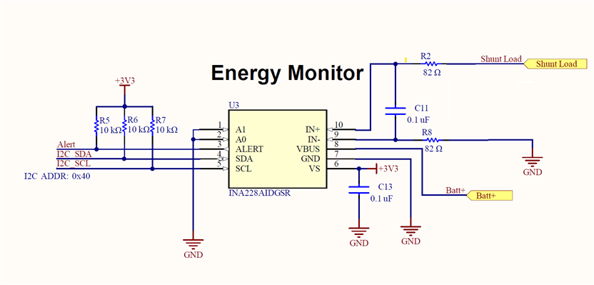
I am experiencing an offset to expected current readings and am having difficulty understanding where they may be introduced from. With current from -10A to +10A, the offset is consistently around -200mA. The amplifier is being used in a low side measurement configuration on a 500A battery shunt. The traces are about 1 inch each to the kelvin connections on the battery shunt (between GND and Shunt Load on Schematic)

Shunt resistor = 0.1 mΩ

SHUNT_CAL = 1280

VBus = 12V

Schematic:

Any insight as to where this offset may be coming from would be much appreciated!

  • Hello Mike,

    Thanks for using the TI forum. I would suggest temporarily removing and shorting where you have the 82Ω input resistors, to see if these are causing the problem.  If these resistors are not matched very well, then it can cause errors, so it would be good to rule them out.  If they end up being the error source, then you can try to find higher precision resistors or lower the resistance value.

    If that is not the problem, then send me a register dump for a known current setting so that I can look into that as well.  

  • No change shorting the 82Ω resistors. INA228 register values below for VSHUNT = 12V, CURRENT = 0.500 A. Thanks

  • Ok, I will look this over, can you also send me an image of your layout?

  • Yup. Will PM to you.

  • Mike,

    I looked over your layout, and I believe that is where the problem is coming from.  I'll give more specific details to your layout in the offline thread, but in general here is a link to a training video we have for layout best practices: https://training.ti.com/ti-precision-labs-current-sense-amplifiers-shunt-resistor-layout 

  • Thanks for your recommendations MItch. I will look into changing the layout regarding one side of the shunt resistor connected to the ground plane. I understand how that is an issue, however how would that be responsible for the offset when zero current is flowing? 

  • I'm thinking this is one of 2 things. It could potentially be from the GND plane, based on the total system and other devices drawing current, but it could also be from thermal changes between different metals from the external shunt connection (seebeck effect). It is hard to say for 100% certain though at this point...  I recommend first making the other changes and seeing if that fixes the issue. If it does not then come back here and we will see if we can think of some other tests to run to help figure it out.

  • I used a scalpel to slice traces into the board and remove IN+ connection to the GND plane. The traces are much closer to equal between shunt resistor and IN+, IN- pins. I don't see any major changes from doing this. To test if the INA228 current offset is caused by the Seeback effect, would it be safe to say that the offset should vary with ambient temperature? When heating or cooling the Shunt resistor, if the offset varies then that would confirm the seeback effect to be the source of error?

  • Hey Mike,

    The easiest way to test the Seebeck Effect would be to just heat or cool only one side of the connection (where different metals are touching) and see if that makes a difference. (To see the offset you are looking at, that would only be 20µV difference).

    A few other notes though.  I was looking more at your settings that you are using, and it looks like if I use the ENOB table in the datasheet and convert to Amps, you have a effective noise free resolution of about 93.3 mA, so 200 mA offset error is only about 2 noise free effective bits. To test the system setup, you may want to increase the conversion time and averaging to maximum to get a better measurement of what is going on. 

    One more thing to check would be to make sure there is no leakage current that the device is measuring, but this can be hard to find...

  • Hi Mitch,

    I've tried heating and cooling the Shunt resistor to test if the Seeback effect is the cause. It might be a small contributor (+/- ~1 mA change over 20 degrees C) but it doesn't look to be the primary source of the offset error I am reading.

    Thank you for pointing out the ENOB, turns out that was an error in my code. Readings are much more stable now, but still offset -200mA.

    I'll start working away to try to locate any possible leakage current by isolating components in my circuit. Let me know if anything else comes to mind I should check.

    Thanks for all the help so far.

  • Hey Mike,

    Ok, so in that case it is likely leakage current somewhere. You could disconnect the load (but leave the shunt connected) to see if the leakage current is coming from the PCB or the load. If the leakage current is always the same, then you could calibrate it out, but it would be hard to know if it will be the same when we don't know the source...  

    You could also get an EVM and measure your shunt with it, that would help show if it is on your PCB or load.

  • I confirmed that the reading offset is caused by leakage somewhere else on the PCB. By soldering connections directly to the INA228 IN+ and IN- pins and running them to the shunt resistor kelvin connections, the current reading was much more accurate. Thanks for all your help.

  • Great! Glad you were able to confirm it!