This thread has been locked.

If you have a related question, please click the "Ask a related question" button in the top right corner. The newly created question will be automatically linked to this question.

LF412-N: Output swing to maximum voltage

Genius 9880 points

Part Number: LF412-N

Hi,

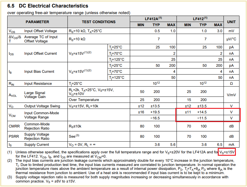
Customer build a simple voltage follower (buffer) circuit using the LF412CN however they observe that the output hit compliance (Max Vcc Voltage) after they adjust the input voltage below 1V (all behavior is normal above 1V). 

They want to know if this is normal or the device is defective. They encountered this in all the LF412CN batch.

Regards,
Maynard

  • Maynard,

    This is normal operation for this device. The valid common mode range is VEE + 4V to VCC - 4V.  In other words, the input is not rail to rail.

    What is supply voltage? We have many other op amps that would work below 1V. 

  • Hi Maynard,

    Yes, with a bit luck, this would work up to an input voltage of +14.5V, for typical individuals. But for other individuals it will only work for an input voltage below +11.0V.

    Kai 

  • Hi Ron and Kai,

    Thank you for your response. Customer want to know why only happen below 1V the output will swing to the maximum voltage? assume the V+ is 5V and V- is GND.

    Regards,
    Maynard

  • Hi Maynard,

    a supply voltage of +5V single supply is way too low for the LF412-N. According to figure 3 of datasheet the minimum supply voltage would be +/-5V. This makes sense because of the common mode input voltage limitations. Remember that the input voltage must stay 4V away from the supply rails.

    Kai

  • Maynard,

    The answer is in the schematic.

    Q4 and Q5 need to be on to keep output linear or VOL. requires  2 VBE (about 1.3V at Q4B)

    When IN+ pin is below 1V, the gate input transistor J2, will become forward biased and source current flows out the gate pin. So Q4 and Q5 turn off making the output high.