- Ask a related questionWhat is a related question?A related question is a question created from another question. When the related question is created, it will be automatically linked to the original question.
This thread has been locked.
If you have a related question, please click the "Ask a related question" button in the top right corner. The newly created question will be automatically linked to this question.
OPA4188_config1.TSCOPA4188_config2.TSCOPA4188_config3.TSC
Hi,
I was performing noise analysis on below circuit using different configurations and hoping to match with the hand calculations, but it looks like I am missing something important.
Reference for calculation: "8.9 TI Precision Labs - Op Amps: Noise - Lab"
Config 1:
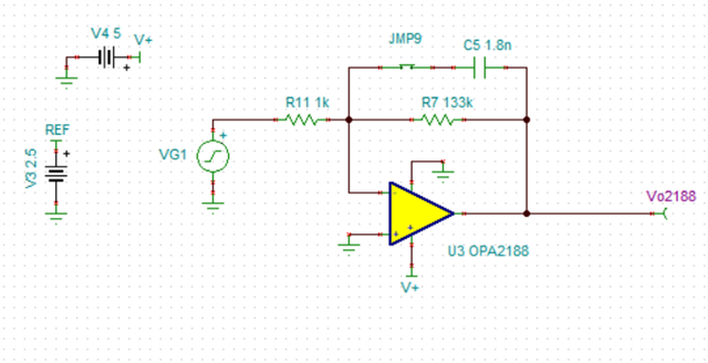
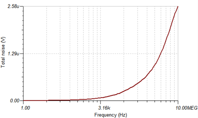
The results of hand calculation are matching with simulation as Vrmsnoise = 1.76uVrms
However, in the referred video, I noticed that, for thermal noise calculation only Rin is considered, not equivalent resistance. Can you please explain why?
Config 2:
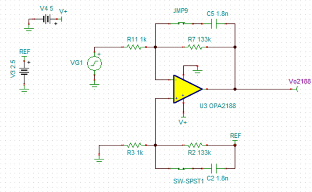
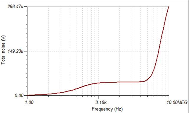
Here RMS noise shot up to 298uVrms.
1. I ran simulation till 10MEG, however if I increase the frequency, noise is still shooting up. Since the cutoff or BWn came around 1KHz, I have considered to run it till 10MEG. Any thumb rule for considering the maximum frequency based on BWn value?
2. I also noticed that if I reduce the REF voltage from 2.5, the total rms noise is reducing. However not able to correlate it to the calculation?
I made two changes, one added differential input configuration and second, added reference or dc offset to that. How do I correlate it in the calculation?
Config 3:
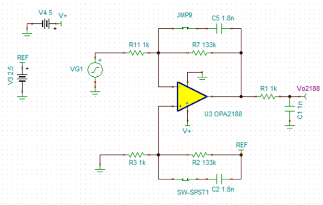
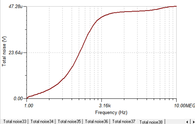
In this, external RC is added of cut off 159KHz and total rms noise reduced to 47.28uVrms.
Noise contributed by o/p RC stage would be:
e.n_r1k = √4.K.Tn.R = 4.05nV/√Hz
Since output RC has one pole, correction factor k = 1.57
BWn = k.Fc = 1.57 x 159kHz = ~250kHz
E.n = e.n_r1k * √BWn = 2.02uVrms
If above calculation is correct for external RC filter, how should I include it to achieve total rms noise = 47.28uVrms
Thanks in advance!
Regards,
Sunney
Sunney,
Please see my comments below:
Config 1.
The results of hand calculation are matching with simulation as Vrmsnoise = 1.76uVrms
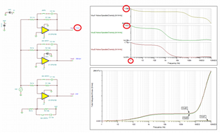
This is not correct since Vout1 is slammed against negative rail - see below Vout1=7.7mV while linear range shown in AOL is at least 100mV above (V-).
You may convince yourself that your circuit is not working linearly by looking below at Vout1 spectral density at 1Hz showing 1.59nV/rt-Hz (???).
Since Fig 17 in datasheet show OPA188 INPUT spectral density of 11nV/rt-Hz @1Hz, the total spectral density at the OUTPUT must be Vout2(@1Hz) = (11^2+4^2)^.5 *(1+133k/1k) = 1.57uV/rt-Hz where 4nV/rt-Hz is noise of Req of ~1kohm - this is close to 1.61uV-rt-Hz shown in Vout2 below and 1000x of 1.59nV/rt-Hz shown in Vout1.
However, in the referred video, I noticed that, for thermal noise calculation only Rin is considered, not equivalent resistance. Can you please explain why?
Since Req=1k||133k = 992ohm=~Rin and thus Req=~Rin may be assumed to be the same
Config 2:
Here RMS noise shot up to 298uVrms
This is correct as shown in my simulation of Vout 2 above.
1. I ran simulation till 10MEG, however if I increase the frequency, noise is still shooting up. Since the cutoff or BWn came around 1KHz, I have considered to run it till 10MEG. Any thumb rule for considering the maximum frequency based on BWn value?
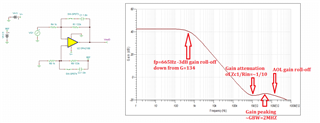
Integrated noise increases beyond fp1 of 665Hz because the noise continue to be integrated at lower and lower gains above fp1 - see below. At 665Hz you have -3dB fp a roll-off of the gain down from G=134 until feedback caps impedance dominates resulting in G=~1/10. Then you have gain peaking around GBW=~2MHz and AOL roll-off at higher frequency - see below.
2. I also noticed that if I reduce the REF voltage from 2.5, the total rms noise is reducing. However not able to correlate it to the calculation?
I made two changes, one added differential input configuration and second, added reference or dc offset to that. How do I correlate it in the calculation?
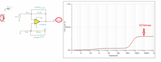
There is no effect of REF voltage or offset on rms noise UNLESS it forces the output to be too close to negative rail - this happens around 60mV (see below).
Config 3:
In this, external RC is added of cut off 159KHz and total rms noise reduced to 47.28uVrms.
This is correct.
Noise contributed by o/p RC stage would be:
e.n_r1k = √4.K.Tn.R = 4.05nV/√Hz
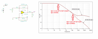
It's not just the noise of the output resistor that gets integrated beyond second pole, fp2, but the total noise including op amp noise - see below.
Since output RC has one pole, correction factor k = 1.57
The circuit has more than two poles - see above.
BWn = k.Fc = 1.57 x 159kHz = ~250kHz
E.n = e.n_r1k * √BWn = 2.02uVrms
If above calculation is correct for external RC filter, how should I include it to achieve total rms noise = 47.28uVrms
The above calculation is far from correct - in order to integrate the total noise you would have to account for changing output noise spectral density resulting from changing gain over frequency - see below. This is not easily done by hand calculation and for this reason we have simulation tool to help us with the task.
