This thread has been locked.
If you have a related question, please click the "Ask a related question" button in the top right corner. The newly created question will be automatically linked to this question.
Hi,
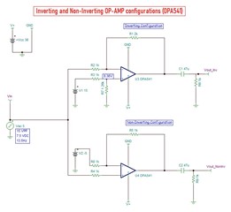
As per the information from the datasheets, I was using OPA 541 in the Single Supply configuration (+36V and GND). But in order to get the proper output, I need to apply biasing voltage at the input terminals of the Op-amp. Especially in the non-inverting configuration, I need t to apply -5V (V2) in the inverting pin. If I'm using a -5V in the circuit, then there is no advantage in going with the single supply configuration. Any solution to replace this -5V.
Thanks in advance.
Hello Sujith,
I set your OPA541 circuit up in TINA-TI to check the DC node voltages as a first step. Below you can see what I obtained. Please check and make sure the voltages are what you expect from your design. A quick check of the voltages applied and the stage gains made on paper agree with the TINA voltage results.
If the -5 V source is indeed required at the upper OPA541 non-inverting voltage path that might be satisfied with an inverting voltage DC-DC converter, which would take a positive supply voltage and invert it to a negative voltage. The downside is it would require an additional IC and its several passive components.
Regards, Thomas
Precision Amplifiers Applications Engineering
Thank you Thomas for your valuable reply.
These were the requirements;
The input signal (sine wave) has a frequency of 13.5Hz with a VPP of 15 volts. It also has a DC level of 7.5V. This signal is passing through inverting and non inverting amplifier configuration at the same time. (Both these configurations have gain 2).
The following is the expected output.
I'm, attaching a TINA design file with this reply which is done using OPA549. We are getting the required output while using OPA549. But when we replaced it with the OPA 541 the output changes. The biasing conditions are the same.
Hi Sujith,
You did change the circuit a bit from the first one. The -5 V source was removed from the input circuit of the lower op amp input circuit, and the resistive divider values were changed in the upper op amp input circuit. The DC output voltages obtained with those two changes would result in a both op amp outputs being at approximately +15 V as the simulation indicates.
The issue that you will run into with any operational amplifier, OPA541 or OPA549 included, is they have a limit as to how close to the supply rails the output can swing. The clipping in the waveform indicates that the output can't swing any closer to the negative rail. How close they can swing is affected by the load current they are asked to deliver. The higher the load current the further from the rail the maximum will be. If you need the amplifier to swing all the way to 0 V, then the V- power pin would have to be powered by a negative supply several volts below 0 V.
Regards, Thomas
Precision Amplifiers Applications Engineering
Hello Sujith,
Do you understand my explanation? Do you have any more questions about your OPA541/OPA549 circuits? If you have the information you need please go ahead and close this e2e thread.
Thanks, Thomas
Precision Amplifiers Applications Engineering