Other Parts Discussed in Thread: OPA2197, OPA2397, OPA197
Dear experts,
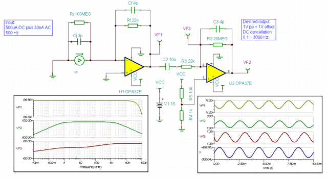
My project requires to interface a weak photodiode signal for further digital acquisition and processing. The useful current produced by the zero-biased photodiode will consist of a mere 30nA, merged in a 500uA DC component (constant illumination, slowly changing during the day). The desired bandwidth lies between 0.1Hz to about 3kHz, power supply is not an issue, nor is components choice. Ideally, the output peak-peak voltage should be around 1V, with a 1V offset, yielding a 300MA/V transimpedance conversion.
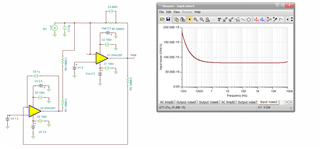
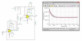
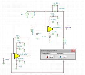
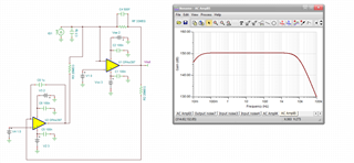
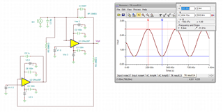
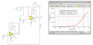
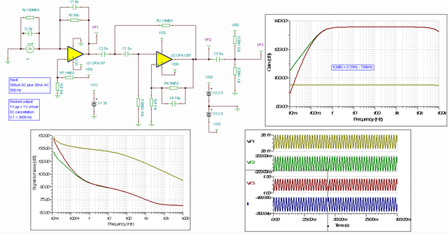
Such high-gain and DC-rejection TIA have been implemented in 3 ways:
- A regular low-gain TIA followed by a high-pass amplifier (current solution)
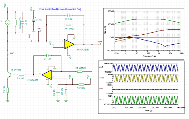
- A single stage DC-servo out TIA with BJT, as well described in Application Note SBOA324
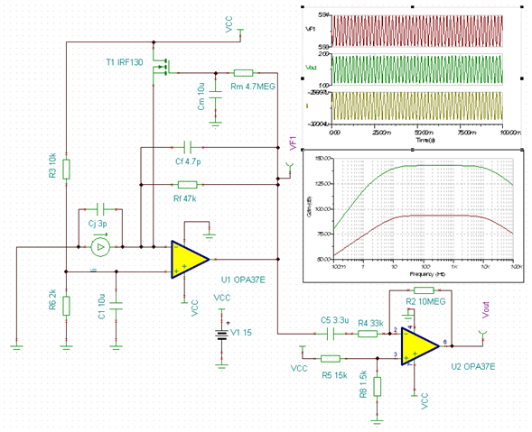
- A DC-servo out TIA with MOSFET followed by a high-pass amplifier, as proposed by Andreas Glatte
Schematics, AC-analysis and traces are enclosed below. Each solution has its pros and cons, and advice on OP-Amp selection, stability or other solution are welcome.
- Two OP-Amp solution induces more noise and a mediocre bandwidth
- BJT servo-out uses a single amplification stage but requires ridiculously large capacitor/resistor
- MOSFET servo-out circuit bias the photodiode (to be avoided)
An extra circuit and photodiode dedicated to DC-component analysis and cancellation may be considered for an improved solution.
Sincerely
1) 
2)
3)