This thread has been locked.

If you have a related question, please click the "Ask a related question" button in the top right corner. The newly created question will be automatically linked to this question.

TLC3704: Dual Power supply

Part Number: TLC3704
Other Parts Discussed in Thread: LM311, LM6511, LM2903

Hi, 

Can TLC3704IPWR be used in dual power supply configuration of +/- 3.3V or +/-5.0V

As VOL = is mentioned as 400mV max and also application circuits or test circuit voltage is considered as VDD = 5V. 

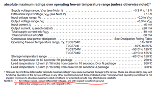
Also there is note mentioned under absolute maximum ratings table that 

"1. All voltage values, except differential voltages, are with respect to network ground." as shown below.

If this part can be used for dual power supply of +/- 3.3V or +/-5.0V (where total acceptable voltage is still less than 18V. Please let me know the VOL in that case.
Thanks & Regards,

Sunney

  • Yes.

    From the point of view of the TLC3704, ±3.3 V is the same as 6.6 V, and ±5 V is the same as 10 V.

    For other supply voltages, the typical VOL is shown in figure 14; there are no guaranteed maximum values.

  • Hello Sunney,

    As Clemens stated, it can be used with split supplies.

    The output will swing -3.3V to +3.3V, or -5V to +5V. (V- to V+). It will not swing from 0V (GND).

    Note that the input range will be Vdd to Vcc-1.5V, or -3.3V to +1.8V or -5V to +3.5V.

    If you need a device that will swing from GND (0V) to a positive or negative voltage, see the LM311 or LM319 or LM6511.

  • Hi Paul,

    Thanks for response. However, to make myself clear, I want to dot all i's and cross all t's. Please verify my responses against your comments.

    The output will swing -3.3V to +3.3V, or -5V to +5V. (V- to V+).

    Comparator TLC3704 can be powered up by the following combinations:

    V+ = +3.3V or +5V & V- = -3.3V or -5V

    It will not swing from 0V (GND).

    If V+ = 3.3V and V- = 0V; then output will not swing from 0V to 3.3V but will swing from VOL, correct? Is that you mean by “will not swing from 0V?

    Note that the input range will be Vdd to Vcc-1.5V, or -3.3V to +1.8V or -5V to +3.5V.

    As per datasheet, input voltage swing V.ICR is 0V to (VDD − 1.5) which means for

    +/- 3.3V power supply -> V.ICR is   -3.3V to +1.8V

    +/- 5.0V  power supply -> V.ICR is  -5.0V to +3.5V

    I think in your example Vdd is negative power supply and Vcc is positive whereas in datasheet only Vdd is mentioned.

    Also, If the input (at either Vin+ or Vin-) is outside the V.ICR then what will be the impact on output?


    If you need a device that will swing from GND (0V) to a positive or negative voltage, see the LM311 or LM319 or LM6511.

    Sure, thanks for suggesting

    Regards,

    Sunney

  • Hi Clemens,

    Thanks for response.

    Sunney

  • Hello Sunney,

    Sorry...got VDD crossed-up. I was looking at a different quad pinout.

    Pin 3 is the positive supply (V+ or Vdd) and "GND" (pin 12) is the negative supply (V-)

    The TLC3704 is a push-pull output, that will swing from the applied positive supply (pin 3) to the applied negative supply (pin 12). It will NOT swing to the mid-supply (GND in the assumed splits supplies).

    This device was assumed to be used in single supply applications, so the "V-" pin is labeled "GND", which can be confusing in a split supply application. When using split supplies, the GND pin (pin 3) is tied to V- (or whatever you want to call the negative supply voltage).

    The output is indeterminate when either or both inputs are outside the V.ICR and we make no assumptions on the output state.

    Assuming pin 3 is the positive supply (V+ or Vdd) and "GND" (pin 12) is the negative supply (V-):

    V+ = +5V and V- = -5V, the output will swing from -5V to +5V, and input range is -5 to +3.5V.

    V+ = +3.3V and V- = -3.3V, the output will swing from -3.3V to +3.3V, and input range is -3.3 to +1.8V.

    V+ = +3.3V and V- = 0V, the output will swing from 0V to 3.3V, and input range is 0V to +1.5V.

    Of course, the above neglects the output voltage drop, which depends on the load (as shown in figures 12 through 15).

  • Hi Paul,

    I am opening this thread again as I have follow up questions:

    1. Since the existing design is working fine even if V.ICR is violated, that led me to do more digging and I found on e2e forums that if one input is with in the V.ICR, comparator will work fine.

    https://e2e.ti.com/support/amplifiers-group/amplifiers/f/amplifiers-forum/434936/lm2903---output-behavior-at-vcc-vicr-2-0v

    Also the comparator in question is different in the post i.e. LM2903

    2. There is another post which is related to TLC3704, which suggests that the comparator might still function in grey area but with degraded parameters like input offset.

    https://e2e.ti.com/support/amplifiers-group/amplifiers/f/amplifiers-forum/746618/tlc3704-recommended-common-mode-voltage-limits

    This brings me to question that, the input we are talking here is the THRESHOLD value of comparator or the other input signal which is compared against threshold or both.

    Lets say if I have TLC3704 with +/-3.3V power supplies, then V.ICR = -3.3V to 1.8V

    At Inverting terminal, input is sin wave of +/-3.3V

    At non inverting terminal, threshold is set to +/-32mV with the help of hysteresis (+ve feedback)

    Then the above design will work or not considering one input is still with in valid V.ICR

    3. "One input valid or with in V.ICR" statement holds true only for LM2903 comparator or specific ones?

    Regards,

    Sunney

  • The LM2903 and TLC3704 have different input circuits. Drawing conclusions from the LM2903's behaviour is not helpful.

    For the TLC3704, there is no guarantee that it will work if one input is outside the VICR.

  • Thanks Clemens for your continued support and that is a key point.  These devices cannot be assumed to be similar and for warranted response, you need to keep the comparator inputs within the recommended operating range.  

    Sunney

    I realize that this is a frustrating point.  There are instances where typical devices will appear to work at conditions outside what is specified in the datasheet but at process and temperature extremes, performance can change.  We do our best to put boundaries around the conditions where proper device performance can be expected.  Operating outside of these areas is not supported with characterization data, so we really can't provide much advice when operating at these levels.

    Chuck

  • Thanks Clemens and Chuck. 

    Yes that was the reason I asked this question as few legacy design are working fine with input being beyond V.ICR however to change the design as per datasheet recommendations I was looking for some rationale how to reason with the arguments.

    I agree with you guys that every part is different based on their internal circuitry and can behave differently.

    Also device performance will be unpredictable if operated against the recommended values.

    Thanks again for your help!

    Sunney

  • You are very welcome and thanks for your post.

    Chuck