This thread has been locked.

If you have a related question, please click the "Ask a related question" button in the top right corner. The newly created question will be automatically linked to this question.

THS7530: output noise single output

Part Number: THS7530

Hello,

I'm trying to simulate output noise on a single output (not differential noise) of THS7530 but I don't understand results.

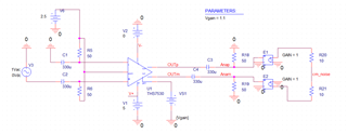
Simulation schematic is below:
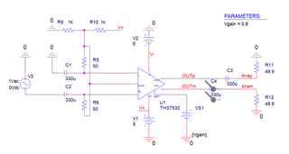
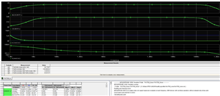
Noise at OUTp at 1MHz is about 139.9 nV/rac(Hz) for a gain of 33 dB. Input noise in this cas is about 3 nV/rac(Hz).
In the datasheet, the input noise curve is below:
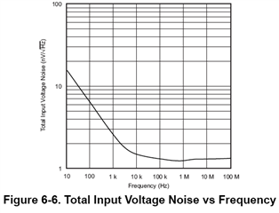
Input noise is about 1.2 nV/rac(Hz) at 1MHz.

So or the noise gain is not the same as the signal gain of 33 dB in my case (but I'm not able to calculate the NG for THS7530 because the loop is inside the component) or the noise is not include in the spice model.

Could you explain me what is wrong, please?

  • Hi Matthieu, First, this graph was taken at maximum gain (46.5dB), and this device uses a Gilbert cell, which does not work the same as a normal op-amp input. Second, the external resistors will add broadband noise, and usually this is calibrated out of the noise presented in the datasheet. Third and finally, the single-ended noise actually should be sqt(2) times higher than differential noise. Noise sources add in series, but they average out in parallel, which is one of the benefits of FDAs.

    Best regards,

    Sean

  • Also Matthieu, looking at your schematic, you might try to put a large cap at the DC reference junction to filter the 1kohm R noise. You have essentially injected their noise in as a common mode noise on each side - and, since you are looking single ended, that adds to what you simulate. Filtering it should reduce your sim output noise. 

  • Actually, looking  back towards the sources - if they are zero ohms this CM noise should not matter. 

  • But to continue that idea, you might try to simulate the output common mode noise and then recognize that is part of your single ended measurement. I would use dependent sources off of each output to a 10ohm divider then measure the noise at that midpoint. 

  • Hi Sean,

    For the gain of the graph, I agree and with same gain, results seem better.

    For the external resistors, I made some tests before my post and I made them again, 1 KOhms on Vocm setting and 50 Ohms on the inputs doesn't change results in the simulation.

    For the differential noise, I agree that common mode noise will be removed using both outputs instead of only one but why using single output will increase by sqrt(2) the noise since noise source on both input will be uncorelated?

    Thanks

  • Hi Michael,

    Thanks for your feedback.

    Same as my response above, 1 KOhms doesn't change any results.

    Could you explain me why by putting 0 Ohms source CM noise dosn't matter?

    I tried to measure the output common mode noise with schematic below (I'm not sure this is OK):

    Noise at cm_noise is 122.3 nV/rac(Hz) while noise at OUTp is 122.6 nV/rac(Hz) so it seems all noise is common mode but regarding differential noise, result is 244.7 nV/rac(Hz).

    Regardind the model, noise seems not modeled (no diode for example) but noise curve are the same as the DS so perhaps model is like a transistor model and so noise will be OK.

  • Parallel (differential) amplifier noise is like parallel resistor noise. The noise is uncorrelated, but it will average out in parallel, not add.

  • Hi,

    Thanks for explanation. I modified eval kit of THS7530 in order to have the same schematic as in the simulation. I measure the noise and it is very nice and seems correspond to simulation.

    Nevertheless, I have an issue with the board. By setting the gain at its max value, output is oscillating around 920 MHz (I need to measure again because my scope is only 1 GHz).

    Because loop is inside the component, why I have this oscillation and how I can avoid it?

  • Hello Matthieu,

      That is strange, because as you said, most of the circuitry is internal and are using our EVMs. Is this only occurring at the max gain (VG+) set to 0.9-1V? Try disconnecting or terminating the input to rule out capacitance from cables. Are R9 and R15 still populated? Also, how are you measuring the output signal (on board sma connectors vs scope probe)? 

    Thank you,
    Sima 

  • Hello Sima,

    Oscillation start at VG+ close to 0.6V but I powered the board at 4.5V (batterie powered), I will try with 5V power supply.

    Input SMA are connected to ground by 50 Ohms directely. R9 and R15 are not populated because I replaced than by output capacitors and I connect the scope using SMA.

    I will also check all my modifications because I have some short wires.

  • Hello Matthieu,

      Thank you for providing the additional information. The issue is most likely using battery powered rather than a power supply, especially since the issue only arises at higher gains. However, usually, this presents itself as lower frequency oscillation which bypass and ac coupling would have suppressed. If first changing supplies, then changing cables do not work, then try setting the EVM in this configuration:

       The isolation resistors will help if there are load capacitances, and 0.1uF would be set by the AC coupling selection of the scope.

    Thank you,

    Sima 

  • Hello Sima,

    Sorry for the delay, I was involved on other subjects.

    Powering the board by power supply and add decoupling doesn't change anything in my issue. I also added serie output resistor (50 Ohms not 25 Ohms) without sucess.

    Nevertheless, oscillations disapear if I change my 330µF tantalum serie input capacitors (C1 and C2 on the schematic above) by 100nF ceramic capacitors. I'll try other value or technologies but do you have an explanation about that?

    Thanks

  • Well Matthieu, 

    What you are describing sounds like an input stage emmitter follower oscillation - if you present a reactive source Z at the base of an emmitter follower that can give a self oscillation at very high F. Your higher blocking C probably had a higher L component. Often, I will add a 20ohm series input R right at the pins to de-Q the resonance of the source C. The schematic I see shows a shunt 50ohm back to a 2.5V reference that should have bypassed the C resonance - but, if that also actually goes resonant above 500MHz, might be gone by the time it matters. 

    This kind of thing is not in the TINA models, we can see it in the full cadence designer sims sometimes. 

  • Hello Matthieu,

      Michael already gave really good suggestions and pointed out resonance due to LC. We opt for ceramics rather than tantalum in higher frequency designs, due to ceramic's lower inductance and high frequency filtering. Here is an app note on decoupling capacitors for high speed amplifiers.

    Thank you,

    Sima  

  • Hi Michael,

    Thanks for this very good explanation, I'll will try with multiple ceramic capacitor instead of tantalum (because I want a low frequency cutoff).

    About the 50 Ohms back to 2.5V, they aren't direcly connected like the schematic but they are connected to the center point of a 1 KOhms resistor divider.

    I'll continu my tests and let you informed.

    Thank you

  • Hi Michael.

    I added a 25 Ohms serie resistor and oscillation disappeared so it seems you are right about the reason.

    Thanks a lot

  • thanks for confirming the fix,