This thread has been locked.

If you have a related question, please click the "Ask a related question" button in the top right corner. The newly created question will be automatically linked to this question.

LMV324: DC offset and output gain

Part Number: LMV324
Other Parts Discussed in Thread: LMV358A, LMV358, TLV9064

Dear team, 

My customer would like to use LMV324 for their application like below schematic. But I don't understand TINA simulation result. Would you please review below schematic and test result? 

- I used LMV358A TINA mode because there is no TINA model for LMV324. 

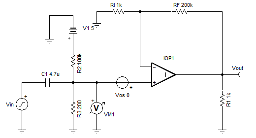
- Schematic is below.

   => Gain 201v/v, DC offset on positive terminal : (0.2K/100.2K) x 5V = 10mV , input Vpp = 10mV 
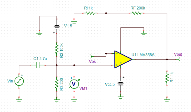
Q1] Please review above schematic and let me know your opinion. 

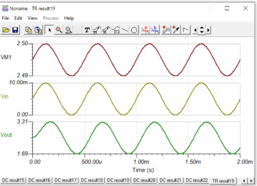
Q2] I expected DC offset of VM is 10mV but TINA simulation result is 4.72mV not 10mV like below.  Please let me know your opinion why the expected value doesn't come out.
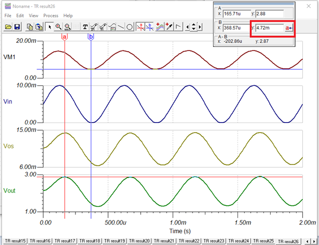
Q3] I expected vout is 2.95V but result is 2.88V.  Please let me know your opinion why the expected value doesn't come out.

Please review above simulation result and let me know your opinion regarding simulation result.  schematic error, setting error or Did I make a mistake some others?

I attached my simulation file

LMV324 simulation_Dino_211119.TSC

Thank you. 

  • Hello Dino,

    Let's make the op amp ideal to make things easier. I added a error source "Vos" that can be zero for now.

    The DC operating point (no input signal): the input is 9.98mV and the output is 2.01V

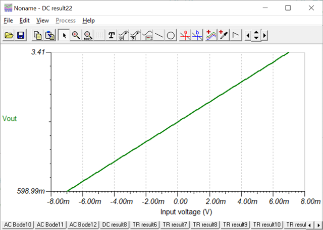
    I believe Vos is going the be the deal breaker, so I simulate Vos between -7mV and +7mV (data sheet range 25C)

    Just from offset voltage alone, VOUT can vary from 0.6V to 3.4V, that certainly is not acceptable 

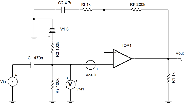
    Adding a cap to 1k will make DC gain become 1 , so Vos will affect Vout by just -7mV to +7mV

    The DC operating point (no input signal): the input is 2.5V and the output is 2.5V

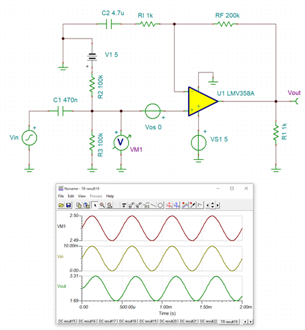
    Lastly, I put LMV358 back in. Now the transient waveform looks like this.

    LMV324 simulation_Dino_2.TSC

  • Hello Ron,

    Thank you for your comment.

    For clarify, there are some questions like below.

    1. You mean the abnormal  DC operating point level is caused by offset voltage of LMV324. Is it right?

    2. I know TINA simulation file include offset specification. Generally, Is it typ value or max value of datasheet?

    3. As you shared the transient waveform like below, Vin peak to peak value is 10mV but Vout peak to peak value is 1.62V. calculation gain is 1.62V/10mv = 162 V/V. Is it also caused by offset voltage of LMV324? please let me know your opinion. 

     Thank you. 

  • Hey Dino,

    1. The abnormal DC operating point is a result of the LMV324 offset voltage, that is correct.
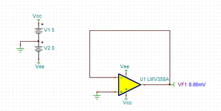
    2. The model can vary as far as what is displayed, typical or max, but in this case you can test this with a simple buffer circuit.
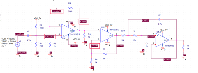
    3. You are not getting the correct gain because you are gain bandwidth limited. 200V/V in one stage is a lot to achieve with one stage. Splitting the gain over two gain stages get you the appropriate output gain. I've attached this circuit below, this isn't optimized and can be tweaked, I just copy pasted the first stage as a proof of concept.

    LMV324 simulation_Dino_3.TSC

    Best,
    Jerry

  • Hi Jerry, 

    Thank you for your comment.but I can't open your TINA file.  more questions. 

    Below circuit is proto board schematic. We will change gain to 2 stage as your recommendation. 


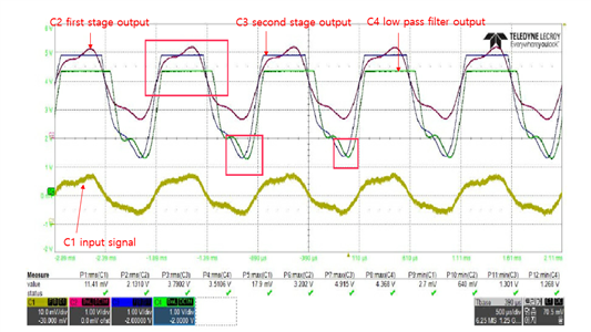
    And below is real board test waveform. 

    In case of C3 second stage output, I knew there is upper limit due to gain and output swing limitation(Max voltage is 4.915V). But For third op amp is used as low pass filter. I think output voltage of third op amp and second op amp output should be the same.

    but why max output voltage is drop to 4.368V(input voltage is 4.915V / second op amp output)? Is this caused by common mode input voltage limit of LMV324? please let me know your opinion. 

    If we change op amp from LMV324 to TLV9064, output waveform is below. there is no output drop. 

    Above TLV9064 waveform, It seems that 3rd amp output(green) is amplified than 2nd amp output(blue).As mentioned above, 3rd amp is used as low pass filter with unit gain. why can I see these results? Is this just output error caused by input offset voltage or bias current? please let me know your opinion.  

    Please review it and let me know your opinion. 

    Thank you. 

  • Dino,

    LMV324 result is a result of input common mode range. 

    Clipping adds a lot of harmonic distortion , so the LPF filtered output won't look exactly like the input.